Hi,
I'm working on the amplifier of a subwoofer (Energy S8.2 , ~ 2002 build date)
(Mods, feel free to move if there's a better subforum)
The amp is fixed now, but I was curious to see how it was designed (class AB MOSFET amp, and an unusual transconductance amp LM13700 !?) so I traced some of the PA board.
I'm not done with the feedback network that involves the LM13700, but the power section should be complete. But part of it is making zero sense to me, despite rechecking the PCB multiple times.
T11 and T9 , current mirrors ?
D15+D16 mounted on the heatsinks, which in conjunction with the pot P3 look a lot like a temperature-compensated bias adjustment.
I can sortof see a kind of differential amplifier combining into T5, but the whole bottom part doesn't work.
T12 tells me "current source", but there's nowhere for the current to go !? Certainly not into T14's gate, and not backwards through D901...
It is not impossible D901 could be a zener (I could only read the last 2 digits "..48" on the glass body so I assumed 1N4148) but that doesn't make any more sense.
Is there anything obvious I overlooked, or some area I should review ?
Or if anyone has a "correct" schem of a similar topology that I could look at for inspiration... but it can't be that hard, this is a 2-layer through-hole PCB...
Attachments
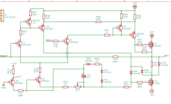
Sadly the schematic is missing quite a few components.
But in general, T6 and T7 look like the input differential pair, you correctly identified them as respectively receiving Input signal and negative feedback, T5 is the constant current source feeding them (into their emitters), T12 could be a Mute or turn-on delay to minimize thump, T9 might be the Vas, the main gain stage, but its load is missing.
IF both Mosfets are same polarity (you sure bottom one isn´t 9640? ... P channel ones often start with the letter P followed by a string similar to the N channel version) then bottom one in general needs a PNP bipolar transistor to drive it and make it behave like a P Channel Mosfet.
IF heatsink mounted, D15-16 might be part of bias, but plain diode voltage drop is too low for typical Mosfet bias needs.
As of LM13700, it is very popular in Compressor-limiters, I might avoid power amp clipping.
Thanks for your comments JMFahey.
I found the problem while replacing some cheezy/questionable caps : one trace connected to V- directly underneath the bulk capacitor. A continuity test would have indicated that but I hadn't tested that particular node yet. Now that whole area just came together : T12 a current source as I suspected, D15+D16 and P3 the bias compensation, and the bottom mofset (indeed an N-channel IRF640, I checked) properly wired now.
I cleaned up the power amp stage a bit and uploaded a second WIP schematic. Still missing all the OTA compressor and feedback network though. It's not clear yet what they're doing with the diode full-bridge (D906,D907 etc) at the bottom left, but as I said this is still incomplete and missing some connections.
That would make sense; the manual does allude to some compressor-like features.As of LM13700, it is very popular in Compressor-limiters, I might avoid power amp clipping.
Attachments
For future reference or others working on these (or the probably similar S10.2 ), I made a quick video with a few notes and comments:
Energy S8.2 subwoofer "repair" - YouTube
Energy S8.2 subwoofer "repair" - YouTube