Hi, i stumbled on a schematic for a class A amplifier with very low output distortuion (0.008% at MAX power).
I picked this schematic from a book, but is seems like there is something WRONG in it!!!!
I built this circuit two times, and two times it had the SAME problem:
When i power the negative rail, the output of the amplifier is just DC voltage. If i power the positive rail, it does not care at all (nothing happens). If i power both, still always DC voltage on the output.
WHY is that!!!?
It's not even built in a prototype board but on a dual layer PCB that i very carefully designed on PC, then i ordered it online.
Two attempts, two failures.
Can you understand if this schematic is actually wrong?
Thank you.
Attachments
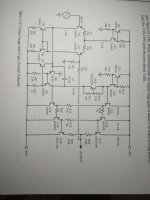

The schematic looks like it would work, but it's missing some vital parts. There's no decoupling for the different stages of the amp. No output inductor of Zobel network either. No input filters also.
The schematic shows designed current flows for the different stages, Have you checked to see if your build matches these? That will point to where the error is occurring.
The schematic shows designed current flows for the different stages, Have you checked to see if your build matches these? That will point to where the error is occurring.
Its difficult to check because all the components are soldered very close to each other.
Why there is just DC current on the output!!?
Is this caused by some missing decoupling capacitors somwhere?
Is there a way to fix it?
All the components i used are identical to the ones of the schematic, even down to the 464 ohm resistor. Yes, its an actual 464 ohm resistor (SMD code 4640). All the transistors are what the schematic suggests.
But if the schematic is wrong is wrong...

Will that solve the problem of DC current at the output? The power NPN transistor heats up A LOT and its 0.33R resistor too.
I'll add the resistor and see if it works.
I'll add the resistor and see if it works.
Ground the input to test. Measure voltage drops on resistors and calculate the current flos from that. Easy to do.
If the input has no path to ground the input stage won't operate. This usually causes the output to go to a high DC voltage.
If the input has no path to ground the input stage won't operate. This usually causes the output to go to a high DC voltage.
Nothing changes, unfortunately. With a higher, lower, directly connected, or no resistor at all to GND the problem remains the same. DC voltage on the output.
I guess the problem lies somwhere else...
I could measure those currents but if i power up the circuit with ±35V it would bake itself in less than 10 seconds...
For testing i'm using just ±10V
I guess the problem lies somwhere else...
I could measure those currents but if i power up the circuit with ±35V it would bake itself in less than 10 seconds...
For testing i'm using just ±10V
Yes but it still heats up way too much, the resistor overheats as well. ±35V is quite a high voltage...
It seems like there are too much problems.
Suggiestions on what should i change to make this work?
If its not worth it then patience but if there is a shot at this, let me know. Thanks.
It seems like there are too much problems.
Suggiestions on what should i change to make this work?
If its not worth it then patience but if there is a shot at this, let me know. Thanks.
This seems to be from Bob Cordell's book (Designing Audio Power Amplifiers). Have you added the input, feedback AC decoupling and output networks from figure 3.16* ?I picked this schematic from a book, but is seems like there is something WRONG in it!!!!
* (in 1st edition)
You have some layout issues with your boards, but you should be able to get this to run as a proof of concept. The amplifier will likely have a lot of supply noise though.
Q10 should likely be mounted on the heatsink. That would be the temperature sensing transsitor for the bias spreader. R11 should be a pot to adjust output stage bias. As is you have no bias control. If you remove R11 the output stage should shut off to make testing possible.
Q10 should likely be mounted on the heatsink. That would be the temperature sensing transsitor for the bias spreader. R11 should be a pot to adjust output stage bias. As is you have no bias control. If you remove R11 the output stage should shut off to make testing possible.
This. Those components aren't optional. The schematics like yours and the other versions in that section are just to illustrate how different topologies affect performance, they are not meant to be complete amplifiers that you can just copy. The minimum you need to at least make sure everything is properly DC-biased are the 19k resistor to ground at the input, the DC-blocking cap before it and the 100u non-polar between R3 and ground (R3 in your schematic, R2 in fig. 3.16).This seems to be from Bob Cordell's book (Designing Audio Power Amplifiers). Have you added the input, feedback AC decoupling and output networks from figure 3.16* ?
* (in 1st edition)
Last edited:
My book is second Edition. It seems like i interpreted everything wrong. That schematic alone probably wont work and needs other circuits attached to it... Sorry. I didnt expect that.
A mistake that i learned from.
A mistake that i learned from.
The posted circuit is meant for simulation or descriptive purposes only and is not complete or intended for an actual implementation due it’s incompleteness.
Funny how op. says it’s from a book and does not disclose what book until the last post.
Chapter 4 is devoted to a complete amplifier design so why did you not use the bc-1 design? Just mod your circuit to match the extra details as used in the bc-1 design
Funny how op. says it’s from a book and does not disclose what book until the last post.
Chapter 4 is devoted to a complete amplifier design so why did you not use the bc-1 design? Just mod your circuit to match the extra details as used in the bc-1 design
Last edited:
Well... What a horrible mistake i made...
I'm just a beginner, after all...
Thank you all for your help.
I'm just a beginner, after all...
Thank you all for your help.
It's also fig. 3.16 in the 2nd edition. I suggest you take a look at the text too in that section (3.12 - Completing an amplifier) to learn what those components do and why they are necessary.My book is second Edition.
Cheers,
Cabirio
I agree wholeheartedly. You've put time, effort and money into that PCB, it's perfectly OK for testing and learning, it would be a shame to let it go to waste...You can likely still make it operate. You can add extra circuits like the input and output filters externally and tack decoupling capacitors onto existing components. You already have them built, no harm in making them run and learning from them.
- Home
- Amplifiers
- Solid State
- Problem with dual supply amplifier (triple emitter follower)