I will check if 50n06 is fake or not. If it is original then i guess it should work just fine.Also, just looked at datasheets... There exists uc384x series without letters, series with A letter at end, with B letter, all specified to handle output of 1 ampere - there should be no problem to drive a mosfet with few nF gate capacity, just decrease gate series resistor.
ok -- continuous
I would drive turn-on slower with 5 to 10 ohms and diode across for faster turn off.
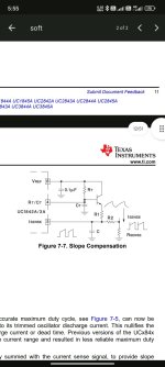
Slope compensation effectiveness depends on max duty cycle. Above 80%, continuous mode subharmonic alternate cycle and RHP instability become much harder to control
I would drive turn-on slower with 5 to 10 ohms and diode across for faster turn off.
Slope compensation effectiveness depends on max duty cycle. Above 80%, continuous mode subharmonic alternate cycle and RHP instability become much harder to control
I agree -- if layout is not right negative spikes can cause IC the latch up or act erratically. 1nF capacitance is nothing for the IC driver so I do not think it is drive strength issue-- in fact adding the 10 ohms with diode as I suggested across should reduce return noise
Please capture drive waveform and drain current when it starts to act up
Please capture drive waveform and drain current when it starts to act up
Ok. I add buffer and same thing happens.
I disagree with layout issues as i have used same for almost 1000 amplifiers and none have failed till date. Using this as 200watt dcdc converter and works like a charm.
And sorry i cannot upload the layout.
I think mosfet might be the issue. But i burnt all which i had while testing. I don't have smd mosfets in stock. And i got those locally which have higher chances of being fake.
I have ordered another lot for testing and they will be delivered after around 12days.
I may be wrong in many ways but the thing is i don't feel to change anything that works flawlessly on field even if that is theoretically wrong. Hope you people understand my point.
Are you saying 1000 amplifiers, or 1000 dc-dc with same control ic and SMPS power conversion level?


I know. I built several amps with irs2092s. And had very much issues that were only related with fake /copy mosfets.
I owned 10 units of 2SK241 MOSFET for an oscillator at 9MHz. Only 2 I used and the same: they catched fire. Another borrowed from an old 50MHz wireless phone oscillates excellent. So my circuit is OK.
Accessing oem components is not very hard but they are priced heavily. For 1-10 nos components versus for 1000nos the price might very 10x.
So for not so demanding or complex circuits people go with cheaper aka fake components.
Dm me with your whatsapp contact. Will be very nice to have a chat with you relating to this topic.
So for not so demanding or complex circuits people go with cheaper aka fake components.
Dm me with your whatsapp contact. Will be very nice to have a chat with you relating to this topic.
Can you capture failure on scope - -- you do not have to download. -- just describe
Trigger on drain current above normal operation to single shot capture failure
Also with good original board what does full load drain voltage and current look like?
Trigger on drain current above normal operation to single shot capture failure
Also with good original board what does full load drain voltage and current look like?
i think my old bosses would have beat me with a stick if I told them I was trying to solve a problem with a supply blowing up without actually knowing what the failure mechanism was first.
I will note that the schematic you posted does not show a gate resistor in series with the FET's gate. 10 or 20 ohms is a typical value. If I remember correctly the resistor stops gate oscillations. Also, this location is used to shape turn-on and turn-off behavior of the FET. The magic in power supply design is all about these parameters. Fast switching improves efficiency, but also drives noise.
I believe an earlier post indicated you are using continuous conduction mode. That is, when the FET turns on there is still current flowing in the inductor and diode. The schottky does not have the reverse recovery issue but it does have capacitance. So the diode goes from having Vforward across the capacitance to having Vout across it when the switch turns on. Charging that capacitance requires current and that current creates noise. Tayloring the turn-on speed of the switch FET to get the right balance between efficiency and noise is what makes power supply design fun.
BTW, the TI webpage shows a newer device, the UCC3802 which has features to resolve issues with the 384x series. You might find the app notes on those issues informative in working with the older part.
Your bosses were naughty i guess😉
Fake fets is my issue i guess. Because the board is used for very long just replaced the fets and boom
Adding old irf3205 will make it work again flawlessly.
So i won't go deep into what the issue is before getting any genuine fets.
Fake fets is my issue i guess. Because the board is used for very long just replaced the fets and boom
Adding old irf3205 will make it work again flawlessly.
So i won't go deep into what the issue is before getting any genuine fets.
I will. I don't have smd fets for the tests now. I blew up every one of what i got locally.
I will do all the tests when i get the fets that i ordered.
I will do all the tests when i get the fets that i ordered.
- Home
- Amplifiers
- Power Supplies
- Problem with DC-DC converter using UC3843