Hi PMA,
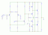
have you thought once about a folded cascode? Your preamp can modified simply: Connect the base of your third bjt to a constant voltage. Remove the resistor from the collector of the second transitor to ground and connect the collector directly to the negative supply.
The benefits of a folded cascode are:
1. Only one amplifying stage
2. Very high cutoff frequency
I like the output stage you made. But it can be made more simple: Remove the output transistors at the right side and connect two resistors (lets say about 470 ohms) from the drivers to the output. I made something similar and found the results very promising.
Hi Pavel
Before I can comment anything I have some questions:
1. What's the RC near diamond buffer? Does it make anthing useful?
2. How do you set low offset voltage?
3. I assume that you are aware that you need very clean rails for your LTP-VAS arrangement and CCSs too, right?
cheers and regards
Before I can comment anything I have some questions:
1. What's the RC near diamond buffer? Does it make anthing useful?
2. How do you set low offset voltage?
3. I assume that you are aware that you need very clean rails for your LTP-VAS arrangement and CCSs too, right?
cheers and regards
Hi bocka and darkfenriz,
B1) The folded cascode is great, I am thinking about comparing more solutions, cutoff frequency of the circuit shown is about 6MHz
B2) I want to keep the lowest output impedance, as I have excellent sound results with it (even if compared to 50 Ohm output impedance)
D1) The RC is a kind of frequency compensation
D2) I do not take into account low DC output offset in this step, this can be solved by standard way (BTW output offset depends on currents through differential pair)
D3) Yes, I am aware of it, again it can be solved by several ways, this is just a concept, which is just able to work
The RC is a kind of frequency compensation
Applied along the section of voltage gain of 1....?
Is it class AB output?
On this RC there is a buffer error voltage drop, dividing by RC impedance you get parasitic error current drawn from VAS.
I think you are trying to be mysterious about the point of this arrangement... This seems to generate more distortion at higher frequencies. Or was it just a cure for non-stability on 6Mhz when strange things do happen?
I think I don't have to say that the rest of the circuit is perfect?
😀
regards
P.S. For some extend your VAS is also folded cascode.
I'd connect pre-out stage transistors collectors to out stage transistors emiters. Such step will make output buffer input impedance significantly more linear.
anli said:I'd connect pre-out stage transistors collectors to out stage transistors emiters. Such step will make output buffer input impedance significantly more linear.
isn't it simply an effect of higher bias?
darkfenriz said:
Is it class AB output?
No, it is class A.
anli said:It is effect of constant Uce for pre-out transistors.
Yes, this is greatly desirable.
anli said:BTW, Pavel, where are emiter resistors for pre-out pair? 🙂
Andrej, where would you like the output transistors to travel? 😉
darkfenriz said:
Applied along the section of voltage gain of 1....?
On this RC there is a buffer error voltage drop, dividing by RC impedance you get parasitic error current drawn from VAS.
I think you are trying to be mysterious about the point of this arrangement...
As you know, the followers have 100% voltage feedback. Do you think they are unconditionally stable?
Pavel,
No, I don't 🙂
There are no resistance values on the schematics. I have suggested output emiter resistors are about 10-50 ohm. In such case to move out stage to class A some emiter resitors are necessary for pre-out pair too. Where is my mistake? Or - what is your concept in words? 🙂
No, I don't 🙂
There are no resistance values on the schematics. I have suggested output emiter resistors are about 10-50 ohm. In such case to move out stage to class A some emiter resitors are necessary for pre-out pair too. Where is my mistake? Or - what is your concept in words? 🙂
Andrej,
you are right. There are no values, which makes the case more interesting. The output emitter resistors are only 2.7 Ohms. Bias current is a game of Vbe voltages and thermal coupling.
you are right. There are no values, which makes the case more interesting. The output emitter resistors are only 2.7 Ohms. Bias current is a game of Vbe voltages and thermal coupling.
With emitter resistors of both 'drivres' and output stage you could add some local modulation or error correction or feedback or whatever one would call it.
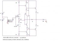
Maybe you would be interested in my use of diamond buffer with modulated current sources (error correction).???
Perfect buffer for unity gain preamp, headphone class A amplifier or filters.
Needs some adjustment of bias and offset: 321R/339R are pots.
What do you think?
schematic:
Maybe you would be interested in my use of diamond buffer with modulated current sources (error correction).???
Perfect buffer for unity gain preamp, headphone class A amplifier or filters.
Needs some adjustment of bias and offset: 321R/339R are pots.
What do you think?
schematic:
Attachments
Forgot to add:
for low power speaker amp/ headphone amp one could take advantage of sweeping bias point.
for low power speaker amp/ headphone amp one could take advantage of sweeping bias point.
You mean to use it as an output stage? The circuit I have shown can have a voltage gain up to 40 dB without problems.
As for preamp (before output buffer) concept, I have selected (and am listening now) this topology:
http://gaydenko.com/preamp/final.jpg
http://gaydenko.com/preamp/final.jpg
Pavel,
I have no experience in listening to nice amps. In such conditions it is the best 🙂
This is card's own spectrum:
http://gaydenko.com/preamp/card-own-4KHz-500mV.png
This is the preamp bridge-half spectrum:
http://gaydenko.com/preamp/un-4KHz-500mV.png
Last one was measured for prototype. In real preamp input fets were selected, and 2d harmonic is about -92db. All others are below my card resolution.
- Status
- Not open for further replies.
- Home
- Amplifiers
- Solid State
- Preamp concept