Hi,
I'm working on a pre-amp and I'm getting close to getting the first boards made up. I'm still new to this and I've had some great advice here before so if anyone has any comments or suggestions for improvement I'd be pleased to hear them. I'm sure many people could design these on two layer boards but I've gone for four layers to help isolate the signal from the DC.
All switching is done by latching relays controlled by an ATMEGA MCU and a pile of TPIC6A595NE high current shift registers. This works great as you can daisy chain the shift registers together, set the values using a serial connection and switch as many relays as you want simultaneously. I've experimented with this setup for switching the gain in my MM stage and I'm unable to detect any switching noise through the speakers (I've not completed the design for the logic board yet - it's a mess of wires on veroboard).
The input board is made up of four RCA inputs and one input for the MM stage I've already built. I couldn't decide on a value for RF filtering so I've made that switchable depending on the output inpedence of the connected equipment. I've also included jumpers to bypass the DC blocking caps if needed. I've used OPA1652s for the MM Stage and was thinking of going for an OPA1612 to buffer the input to the attenuator and keep the resistors low value. I'll use something cheaper to drive the VU meter.
The attenuator can accommodate two input boards and provides 255 0.5db steps (more than I need but doesn't cost much extra). I've been worried about the switching noise so I've included a slave output and input so that if I need to I could stack two boards and route the signal through each board once all the relays are set. Hopefully I won't need to do that.
I'm still working on the output board and logic controller but I thought I'd post these and see if I'm going along the right lines.
I've set up the layers the same on both boards (I've not uploaded pics for layer 2 & 4 of the attenuator as they're just pours):
1 - Signal
2 - Signal Ground
3 - DC Ground
4 - DC Power, decoupling caps for the op amps and flyback diodes for the relays.
Any comments advice greatly appreciated.
Simon.
Attachments
-
Input Schematic.pdf32.8 KB · Views: 278
-
Attn Layer 3.pdf67.1 KB · Views: 69
-
Attn Top Layer.pdf41.6 KB · Views: 97
-
Attn Schematic.pdf36.4 KB · Views: 188
-
Input Bottom Layer.pdf49.4 KB · Views: 74
-
Input Layer 3.pdf75.3 KB · Views: 64
-
Input Layer 2.pdf75.9 KB · Views: 64
-
Input Top Layer.pdf45.2 KB · Views: 96
Thanks. Still working on it, the boards are made up but I've got to get it all in a box. The designs were tweaked a bit before fabrication but the principles are the same as in the original post.
I'm pleased with the attenuator, it was pretty straight forward to get rid of the switching noise without needing to route between two boards. 256 steps was a bit over the top though, I could easily drop the 64dB stage and save on a relay and a handful of resistors.
I'm pleased with the attenuator, it was pretty straight forward to get rid of the switching noise without needing to route between two boards. 256 steps was a bit over the top though, I could easily drop the 64dB stage and save on a relay and a handful of resistors.
I'm pleased with the attenuator, it was pretty straight forward to get rid of the switching noise without needing to route between two boards.
What do you mean by this? What switching noise? Noise in the signal or just noise of the relays?
Initially I was getting a click when switching multiple relays e.g 63 to 64dB, I just added a very small delay between closing one set of relays and opening the rest. The signal noise is very low, I buffered the inputs and outputs with OPA1612s which meant I could keep the attenuator down to about 1k.
Yes, that is the issue with relays - the time to close a relay is generally less than the time to open a relay, so as they settle, intermediate attenuation codes can be asserted, causing signal clicks and random garbage. The best way to avoid this problem is to switch from one code to 'off' and then after a small delay, to the new code, and not go directly between two attenuation codes.
I've attached the schematic and layout for the latest version of my MM preamp design. I've not done a lot of testing on this board but I've been using the previous version for a few months and am pretty happy with the performance. It's a four layer board but I've left the internal layers out of the pdf they are ground planes and routing for the relay switching circuit.
My main worry for this design was the feedback loop area of the final gain stage, this does not appear to have affected the stability of the op amp though. The biggest difference between this design and the previous one is that I've used a log attenuator in the feedback path rather than R2R.
My main worry for this design was the feedback loop area of the final gain stage, this does not appear to have affected the stability of the op amp though. The biggest difference between this design and the previous one is that I've used a log attenuator in the feedback path rather than R2R.
Attachments
As an aside... I had real problems making up this board. Up until now my workflow has been to solder the SMDs then blu-tac the TH components in place prior to soldering those. Everything looked fine but when I ran the first tests I was getting hideous noise and distortion from one of the channels.
I traced the problem down to the relays so I cleared and re-soldered all the pins with plenty of flux... couldn't fix the problem and ended up lifting one of the pads by over heating. So I got out the hot air gun and to recover some of the more expensive components - it was then that i noticed a bit of blu-tac had made its way under the relay case and was shorting three of the pins!... frustrating waste of time but at least I know what the problem was.
I traced the problem down to the relays so I cleared and re-soldered all the pins with plenty of flux... couldn't fix the problem and ended up lifting one of the pads by over heating. So I got out the hot air gun and to recover some of the more expensive components - it was then that i noticed a bit of blu-tac had made its way under the relay case and was shorting three of the pins!... frustrating waste of time but at least I know what the problem was.
All the boards made up and working now, when I was testing the input, attenuator and output in isolation I was getting -113dB THD but when I connected them together I could only get -96dB. After a lot of experimentation I ended up changing the signal cabling from van damme pro-patch to console cable and I'm getting -114dB THD from input to output which is the same as I get loopback testing the QA401.
The noise measurement isn't quite there yet but I'm testing the boards in a rat's nest of wires on my bench - hopefully that'll improve once I get everything in a box.
The noise measurement isn't quite there yet but I'm testing the boards in a rat's nest of wires on my bench - hopefully that'll improve once I get everything in a box.
")
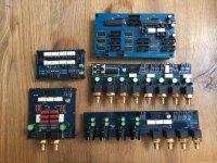
Clockwise from bottom left:
MM Input: OPA1652 based RIAA stage with 35dB gain, followed by a switchable sub-sonic filter and a final 0 to 35dB (in 5dB steps) gain stage.
Attenuator: 0 to -127.5dB in 0.5dB steps, the unpopulated relay positions were to allow switching between two attenuators which I'm no longer planning to do.
Logic board: 2xAtmega328P-PU linked by I2C. I was going to use an ATMEGA2560 but the TH packages worked out easier to route. I'm using a motorised pot as a volume control so one Atmega will control the motor while the other can read the pot and set the attenuator.
Input board: HPF selectable (100pF/780pF) and 22uF dc blocking with a jumper to bypass. OPA1612 as buffer on output. The fuse holders are just there to hold spare VU meter bulbs and next to that somewhere to park spare jumpers.
Output: 2 x balanced with DRV135 and 2 x unbalanced. One RCA is always on the other three outputs are switchable.
VU meter will be switchable between the input board and the output.
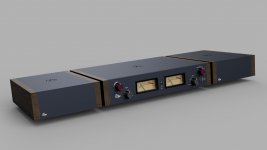
I've also included an image of the chassis design, the two power amps will be parallel LM3886. I quite like the look without vent holes in the top so I may go with forced air cooling if I can get it quiet enough.
Edit: Can anyone spot the schoolboy error on the PCBs?
MM Input: OPA1652 based RIAA stage with 35dB gain, followed by a switchable sub-sonic filter and a final 0 to 35dB (in 5dB steps) gain stage.
Attenuator: 0 to -127.5dB in 0.5dB steps, the unpopulated relay positions were to allow switching between two attenuators which I'm no longer planning to do.
Logic board: 2xAtmega328P-PU linked by I2C. I was going to use an ATMEGA2560 but the TH packages worked out easier to route. I'm using a motorised pot as a volume control so one Atmega will control the motor while the other can read the pot and set the attenuator.
Input board: HPF selectable (100pF/780pF) and 22uF dc blocking with a jumper to bypass. OPA1612 as buffer on output. The fuse holders are just there to hold spare VU meter bulbs and next to that somewhere to park spare jumpers.
Output: 2 x balanced with DRV135 and 2 x unbalanced. One RCA is always on the other three outputs are switchable.
VU meter will be switchable between the input board and the output.
I've also included an image of the chassis design, the two power amps will be parallel LM3886. I quite like the look without vent holes in the top so I may go with forced air cooling if I can get it quiet enough.
Edit: Can anyone spot the schoolboy error on the PCBs?
Attachments
Last edited:
- Status
- This old topic is closed. If you want to reopen this topic, contact a moderator using the "Report Post" button.
- Home
- Source & Line
- Analog Line Level
- Pre Amp & Attenuator PCBs