Amp came in with a multitude of issues. PS fets shorted. PCB un-grounded to case. Main rectifiers broken. 1N4936 rectifiers shorted. R83/R122 'shield' resistors shorted. C13/C21 caps blown, RCA shields detached, and probably several other issues I've missed noting.
Combed through everything I can, and the LEFT channel still has a problem. Under load, sometimes the amp will draw excessively and cause the voltage across output emitters to be excessive.
I carefully serviced the driver board in the Left channel, and then eventually replaced this board with a known good one to no help. I replaced main 2n6487/2n6491 output transistors because I noticed one not matching and that seemed to help just a bit; but did not fix the issue. I pulled, tested, and replaced the bias transistor MPSAxx. Cleaned the bias pots. Also pulled the output buffers (TO-92) and drivers (TO220) and they've tested ok so I re-installed them. The output pre-drivers on the ceramic boards are measuring OK.
The bias pot in the right channel operates fine, but left channel is very sensitive to any change, and then causes the amp to hit my PS current limit. I've measured up 40mv across emitter resistors. The left channel is also very sensitive it would seem to my oscope which gets better if I set the probe to 10x.
I've got current limiting set to 3A. Cold power-up and the amp idles at 1.25A with bias pots CCW. Transistors clamped, loaded channels. Right channel pulls clean to 3A. Left channel starts out clean but after the amp starts drawing about 2A under load the left output transistors pull to the limit with what seems like bias over-shooting. I immediately pull power to the amp when this happens. I then disconnect RCAs and all load within a few seconds and attempt to power the amp back on; but it still pulls hard to the limit. If I wait with the power off for a few minutes the amp will eventually power on no problem, and then repeat the problem if driven with slight load.
Any advice?
Does installing a shunt on the 2-pin bias headers change anyhting?
Are you sure that the problem isn't in the power supply? As the current draw from the outputs increases, the pulse width increases and there's a problem with the PS drive?
Do you have a set of clamps to run the amp the amp without the cover?
Are you sure that the problem isn't in the power supply? As the current draw from the outputs increases, the pulse width increases and there's a problem with the PS drive?
Do you have a set of clamps to run the amp the amp without the cover?
With a shunt on the 2-pin, the amp works fine but with notch distortion. No issues with over-drawing.
Not a problem with limit. The input signal is barely more than idle. Often the amp 'sticks' on and draws with nothing connected.
Yes the transistors are clamped outside the chassis to insulated bars.
Not a problem with limit. The input signal is barely more than idle. Often the amp 'sticks' on and draws with nothing connected.
Yes the transistors are clamped outside the chassis to insulated bars.
Do both channels swing cleanly up to clipping with a load with the shunt in place?
Does it try to draw excessive current at odd times (not corresponding precisely to the output level) when ramping up the signal?
Does it try to draw excessive current at odd times (not corresponding precisely to the output level) when ramping up the signal?
The right channel doesn't need the shunt. Works fine up to clipping 4-ohm load. Draws about 27A at clipping.
The left channel with shunt plays fine up to clipping. ~27A draw. Without the shunt it jams up and draws excessively once it reaches about 2A draw; then pegs to limit. 4-ohm load.
The left channel with shunt plays fine up to clipping. ~27A draw. Without the shunt it jams up and draws excessively once it reaches about 2A draw; then pegs to limit. 4-ohm load.
When the left channel starts to draw excessive current, does the output on that channel remain pure 0v at the reference line?
What did you mean by 'shorted' shield resistors in the original post?
What did you mean by 'shorted' shield resistors in the original post?
Pure zero, you mean no output? No, it plays something actually.
I meant burned open shield resistors. 10ohm units behind the RCAs.
I believe actually theres still an issue either on or possibly before the driver board. The larger pre-drivers if I measure the center legs a sign wave looks a bit warped on the left channel. These pre-drivers also are running about 170F which is about 40F hotter than the right channel; which is clean on opposite center legs.
It's unlikely that 2 driver boards had the same problem.
Does the signal feeding the driver board remain clean?
Virtually all components on the driver board are inside the feedback loop and may not look like audio as it works to compensate for any distortion in the output of the amplifier. The signals may change significantly with nothing more than a change in the load on the speaker terminals.
The large drivers have 100 ohm printed resistors behind them which sometimes fail but it's not likely that 2 driver boards will have precisely the same defect. For the SOT-89 transistors that have an exposed collector on back, the 100 ohm resistor can short to the collector.
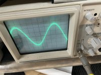
Signal on pins 3 & 4 of the driver board looks clean and identical while the shunt is in. WIth the shunt removed, pin 3 (Input) and back through several ~1k resistors looks very dirty. On the scope looks like some sort of massive ripple
Here are images on R55 with shunt IN (clean) and OUT (dirty)
Here are images on R55 with shunt IN (clean) and OUT (dirty)
Attachments

It's oscillating. That alone could cause the excessive current draw. This could be due to a capacitor out of tolerance or even a leaky transistor.
- Home
- General Interest
- Car Audio
- PPI A600.2 driver/bias problem