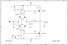
Thought I'd throw this one out for comments, improvements, etc. I built up a prototype of it tonight and it works fine, a little trickey to set up, but once it is it sounds pretty good. My prototype didn't have the grid stoppers or the source resistors. Also I calculated that the parrallel feedback resistors should be about 2.1K. A little less feedback should increase the output, but i havn't experimented to find that threshold point (I.E. Clipping VS not clipping). As it stands I calculated the output @ ~ 60W.
Set up:
Without Output transistors in place, set vr1 and vr2 to the middle position. Adjust these so that the drop across both of them is about 1.7 V (you may have to also adjust the 1K VR to acomplish this). Disconnect power and solder in output transistors. Apply power and readjust VR1 and VR2 to drop 1.7V and have an acceptable offset on the output. This is the trickey part, but possible. For some reason, if I adjusted the drop to >2.3V it seemed to blow the output transistors. I made the PC board with a top ground plane and it might have just been a short circuit from some part touching this ground plane as I tried numerous Resistors of different values to adjust the offset in place of VR1/2 before I decided that it would be easier just to use Variable Resistors. These Resistors 1) Set the bias for the OPT and 2) set the gain for the input stage. The OPT provides gain, so the gain need not be high in the first stage.
I would Like to hear comments. My design critera was to make an all FET amp and to keep it very simple (and PP for heat's sake).
Schematic:
Attachments

Hi Dozuki.
VR1 and VR2 provide two functions in your circuit...the off set null adjustment and the bias current in the output stage...so you must regulate first the bias current in one of this pots and only after that and with the other pot to take care of the off set voltage.
You say that you don't have grid stoppers...but you must use it...if not certanly you will have parasitics oscilations.
One more point...the voltage gain of your amp is + - 5 so for 30 volts peak output you need 6 volts peak input...so you need a high signal to drive it.
For some reason, if I adjusted the drop to >2.3V it seemed to blow the output transistors.
VR1 and VR2 provide two functions in your circuit...the off set null adjustment and the bias current in the output stage...so you must regulate first the bias current in one of this pots and only after that and with the other pot to take care of the off set voltage.
You say that you don't have grid stoppers...but you must use it...if not certanly you will have parasitics oscilations.
One more point...the voltage gain of your amp is + - 5 so for 30 volts peak output you need 6 volts peak input...so you need a high signal to drive it.
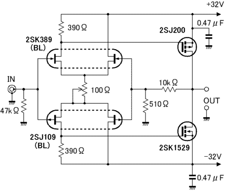
I threw in the fact that the output transistors blew as a side note (not obvious). I suspect it was a short circuit problem more than a biasing problem. The OPT Mosfets are rated at 6A and biasing them at 2v+ shouldn't be a problem. They don't even turn on till they are biased at 1.5V. I will add source resistors and do some measurements later and figgure this one out.
As for not having grid stoppers or source resistors, like i said it was a prototype to work out the schematic. It might have oscillated at higher biases, might not have. Once the bias and offset were set the amp stayed really cool, therefore i didn't worry about oscillations, however i did put these components in the final schematic as the final design will have these. I also forgot to add to the schematic .1uF decoupling caps on the rails. As for setting the bias and the offset - this is a touch task. Slight adjustment of one VR will affect the bias at the other VR and the offset. Not impossible, but a trickey thing with this little circuit.
As for the gain of the amp, a 3 Vpp sine in gives a 31.7 Vpp out. Direct connection to a CD player is plenty of driver for this amp.
-D.
As for the gain of the amp, a 3 Vpp sine in gives a 31.7 Vpp out. Direct connection to a CD player is plenty of driver for this amp
The gain of your amp is given by
1+ (2.100/ 510)= 5,11
Then with 3Vpp you have 3X 5,1= 15,3 Vpp
Something is missing in your calculation...😉
Tube Dude-
My data is not from calculation, it is from actual measurement. The Gain of the Amp is 10, a 3 Vpp sinewave from a test CD gives a 31.7 Vpp output on my OSCILLOSCOPE. Like I said, both stages have gain and the simple calculation of 1+(RNF1/RNF2) obviously doesn't hold true here.
Dshort-
I didn't play a whole lot of music throgh the amp, but when I did, I liked what I heard. Everything was in its places from the highest highs to deepsest lows, and loud to boot (didn't use preamp or volume pot, just straight from the CD player. I suspect that this amp will be a bit particular about speakers, but I don't plan on driving any difficult loads with it. Most of the speakers I build are either single drivers or full rangers with helper tweeters and simple 1st order x-overs.
Dozuki said:Tube Dude-
My data is not from calculation, it is from actual measurement. The Gain of the Amp is 10, a 3 Vpp sinewave from a test CD gives a 31.7 Vpp output on my OSCILLOSCOPE. Like I said, both stages have gain and the simple calculation of 1+(RNF1/RNF2) obviously doesn't hold true here.
Hi Dozuki
Maybe you will win a Nobel Prize ,because you have discouvered something new in electronics:
A feedback amplifier, were the closed loop gain is bigger than the gain given for the calculation of 1+(Rf1/Rf2)....😉
Dozuki - did you actually measure the 3V p-p from the cd player and did you calibrate the o-scope?
dshort-
I have a handheld oscilloscope that reads the AC voltages . Its a single trace, so its only good for rough monitoring work, but I do like that it displays voltages. It will show them as Vpp Vrms or Vdb. I usually do my measurements in Vpp as this makes the most sense to me. The reading of my test CD shows the 1Khz sine as 3.27 Vpp. Using this CD the Oscope shows reading of the same wave @ 31.7 Vpp with the above amp. Therefore the gain as amp stands above is ~10. Chaning the parralled feedback resistors will change the gain. I originaly started off with just the 10K resistor, but that resulted in complete clipping of the amp. To back the gain off I added the 2nd resistor. I just soldered it directly to the PC board, as I was tired of soldering/desoldering the bias resistors. I went out and did some resistance measurements on the pots in this amp and have come up with a revised schematic. This will be my next prototype. In the original schematic the pot between the LTPs was supposed to set the offset voltage. This didn't actually work out, it just raised or lowered the bias in each LTP at the same interval. I would like to also note that I simulated the circuit before I built it. This was good for seeing what happened when I changed values, but real-life values and voltages were WAY different. But, I think that most of us know this.
-D
Attachments
Tube_Dude said:
Hi Dozuki
Maybe you will win a Nobel Prize ,because you have discouvered something new in electronics:
A feedback amplifier, were the closed loop gain is bigger than the gain given for the calculation of 1+(Rf1/Rf2)....😉
this is called positive feedback 😀
I like that circuit.
But is the gain 30 with a speaker load?
Seems to me the input stage has very little gain. Unloaded the output has lots of gain since they are curent source loaded, but with an 4-8ohm load that gain drops a bit???
But is the gain 30 with a speaker load?
Seems to me the input stage has very little gain. Unloaded the output has lots of gain since they are curent source loaded, but with an 4-8ohm load that gain drops a bit???
The more I think...ouch, I think this amp is a bit load dependant, gain rising when load impedance rising. Thats kinda like amps with zero loop NFB, and I'm one of those who believe that's actually a GOOD thing. I'm not even going to try and argue about this, but all amps I've heard it's the amps with this kind of load dependancy that sound best. Oh, oh, dont start this...
Ah, interesting! Who can spot the erroneous premise in TubeDude's supposition?Maybe you will win a Nobel Prize ,because you have discouvered something new in electronics:
traderbam said:
Ah, interesting! Who can spot the erroneous premise in TubeDude's supposition?

Maybe the Nobel Prize should go to this guy here:
http://www.ne.jp/asahi/evo/amp/J200K1529/report.htm
http://www.ne.jp/asahi/evo/amp/J200K1529/report.htm
traderbam said:
Ah, interesting! Who can spot the erroneous premise in TubeDude's supposition?
I'll bite...
I can't imagine any scenario in which this amp doesn't look like a standard negative feedback amplifier. So it's gain can't possibly be above 1/B (~= 4) because that's the limit as Ao gets astronomically large..
Please enlighten us..
--
Danny
Maybe the complementary differential / complementary output thingie doubles the gain
but I'm really not sure
but I'm really not sure
No. They are feedback resistors that estimate the gain. No other way is possible. The gain is less or equal to the 1 + resistor's ratio (non-inverting amp).
- Status
- Not open for further replies.
- Home
- Amplifiers
- Solid State
- PP All FET Amp