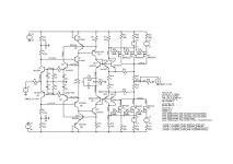
The amplifier has 2 stages: voltage amplifier and current amplifier with each stage having a separate feedback loop. The motivation for removing the overall feedback loop is to reduce the overload of the input stage due to crossover distortion on the voltage amplifier, implemented using IRFP240/IRFP9240 vertical power mosfets biased at relatively low current (100mA). The crossover distortion occurs each time a power transistor turns on. and pushes the gain of the power stage down to cero (close to). When cascaded with the voltage gain stage, the gain is still cero. Independent of the amplifier bandwidth, feedback cannot correct the crossover distortion if the gain is cero. It is difficult to predict the output waveform because the circuit is time-varying. But single inspection indicates that the error signal produced at the input of the amplifier is very large. The resulting transient response at the crossover point shows a large overshoot and ringing that last a longer time than the charge time of the gate capacitance, that means, the time required to have the gain reestablished. By splitting the feedback into two separate loops simulations indicate that transient distortion at the crossover point is reduced both in amplitude and duration. Overall distortion is higher, as circuit theory predicts, but tests show to be below 0.1% at any frequency for this particular circuit. The voltage amplifier is composed of a cascade of a common base input stage and a folded cascode. The power stage, composed of a complementary pair in compound (quasi Darlington?) configuration with single loop feedback (common base - common source), achieves the required unity voltage gain.
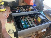
The two monoblocs are build using chassis and power transformer from old PA amplifiers, includes additional capacitors (4 x 4700uF each) on the supply rail, and semi-translucent acrylic front panel for esthetics. Would like to discuss described feedback topology.
The two monoblocs are build using chassis and power transformer from old PA amplifiers, includes additional capacitors (4 x 4700uF each) on the supply rail, and semi-translucent acrylic front panel for esthetics. Would like to discuss described feedback topology.
Attachments

I've been looking at generating a common-mode correction signal to the MOSFETs, so that both MOSFETs always conduct. This correction signal could supply some kind-of overload characteristic, like full-wave rectification, and some trimming may be necessary to ensure it stays orthogonal to a high degree of accuracy so it doesn't distort the output.
A common feedback line would not 'see' this distortion, and would therefore ignore the active bias.
Split current feedback and quasi single-ended also interests me: simulated Exicon MOSFETs can generate >5% THD when measuring output on the source resistor. However, with complementary signals combined on the drain side, the exact same signal only appears to produce <1%. I don't like this over-reliance on cancellation, because it is a recipe for amplitude modulation of the harmonic distortion products. Depending on interactions with other frequencies, the degree of cancellation is modulated. Since many people like to add external sources of harmonic distortion, this suggests that they are actually reducing the amount of modulation by swamping it with steady harmonics. I would like to avoid generating that modulation in the first place.
I've been trying to accomplish some sort of constant (minimum) bias irregardless of signal amplitude with no positive/useful results. The depicted schematic implements an alternative solution, it senses bias current of the output transistor with independence of the temperature dependent gate-source voltage. Comparing the sensed current with a constant independent of temperature voltage results in a constant independent of temperature bias current. Tests prove this correct. But it does not remove the crossover related issues.I've been looking at generating a common-mode correction signal to the MOSFETs, so that both MOSFETs always conduct. This correction signal could supply some kind-of overload characteristic, like full-wave rectification, and some trimming may be necessary to ensure it stays orthogonal to a high degree of accuracy so it doesn't distort the output.
Maybe look at current dumping as implemented in the QUAD 405?
It seems that does what you are trying to accomplish.
Jan
It seems that does what you are trying to accomplish.
Jan
I remember listening the Quad 405 (early 80's?) and some description of the circuit topology regarding a parallel configuration of a low power (current limited?) class A amplifier and a high-power class B. A similar approach was taken by Sansui (except serial, not parallel). The operation of the Quad circuitry is not obvious to me, but I cannot see that it helps in any way to have the power transistors always conducting a minimum current to ease the crossover situation.Maybe look at current dumping as implemented in the QUAD 405?
It is worth to study the '405 principle. For the situation that the dumpers are off (not conducting), the class A directly drives the output.
As the dumpers come on, the bridge topology throttles down the loop gain of the class A amp at just the right value so that the total gain remains the same so there is no gain step or gain doubling and no xover.
In practise, tolerances cause a minuscule wrinkle.
And all that with no adjustment that can be f*cked up or drift over time and temperature.
As I said, worth to study if only to get an alternative view.
Edit: I would say, your goal is not 'always conducting output devices', your goal is 'no xover distortion'.
That may not be the same.
Another interesting study object is the Sandman class S.
Jan
Last edited:
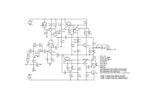
Following your suggestion I searched for the schematic of the Quad 405, and simulated using LTspice. My understanding (probably wrong!) is that the output stage includes a simple VAS, actually sort of primitive implementation using a bootstrap capacitor with split load resistors, driving a complimentary stage using a quasi-darlington instead of a PNP complementary transistor. The output of the VAS connects to the speaker output with a 47 Ohm resistor. The input amplifier and VAS have a low combined voltage gain (~x5), set with a local feedback loop, the rest of the gain provided by the operational amplifier, also in charge of control of DC output voltage (extremely high DC gain). In sum, only a 47 Ohm resistor that connects the speaker output with the class A VAS. Simulation results show some amount (150mV deviation from ideal trace) of crossover distortion. I cannot see any "revolutionary" aspect in this design. I insist, I may be wrong in my personal appreciation of the design by missing to consider some important issues. I include a copy of the schematic used for evaluation.It is worth to study the '405 principle. For the situation that the dumpers are off (not conducting), the class A directly drives the output.
As the dumpers come on, the bridge topology throttles down the loop gain of the class A amp at just the right value so that the total gain remains the same so there is no gain step or gain doubling and no xover.
Attachments
Current dumping still needs a small Class A stage what consume about 1/100 of maximum total current output. For Quad 405, it is about 50mA for the Class A.
Nowadays, a CFP output stage could achieve similar THD figure with less bias.
Nowadays, a CFP output stage could achieve similar THD figure with less bias.
I think the first step should be the basic concept, see attached, instead of diving into the details right away.
Then you can use that for your own design idea if you wish.
Does the attached help? I can post with increasing detail if you want 😎
Jan
Then you can use that for your own design idea if you wish.
Does the attached help? I can post with increasing detail if you want 😎
Jan
Attachments
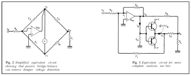
I agree with the simplified circuit you suggested, except the feedback resistor Z1 connects to the speaker output. And Z4 is only a current sensor for the short circuit protection scheme (some miliohms). The presence of Z3 (a feedforward correction?) doesn't seem to reduce crossover distortion. Using the LTspice circuit, moving Z1 from 47 Ohm to 470 Ohm distortion is unchanged ( 0.03%).
No, Z4 is not. It is one part of the balancing bridge.
Try to grok the bridge.
https://www.quad-hifi.info/public/pjw_ww_dec75[3370].pdf
Jan
Try to grok the bridge.
https://www.quad-hifi.info/public/pjw_ww_dec75[3370].pdf
Jan
Z4 is the parallel of a 75 Ohm resistor with a 3 uHy coil, at audio frequencies equivalent to a short circuit. You can also add in series a 0.068 Ohm used to sense short circuit currents. Only on the negative semi-cycle. Some of the older circuits change that part of the circuit but the final result is the same.
Well if you keep on speculating instead of studying the literature, I can't help you.
Good luck.
Jan
Good luck.
Jan
- Home
- Amplifiers
- Solid State
- Power Amplifier using Split Feedback Loops