If we take as an example my usual drivers, 2sb649/d669, which are 20W devices and run them from +-58Vdc. The SOA de-rating allows about 13W when Tc=25degC.roender said:Yes, at least at 15% output idle power
Assuming the heatsink attached to these drivers keeps the case temperature (Tc) to about 60degC, the temperature de-rated SOA is now about 9.4W.
At 58Vdc these powers convert to maximum continuous current of 344mA (20W), 224mA (13W), 161mA (9.4W).
If we take your suggested minimum bias current as 15%, to which current do we apply your factor?
AKSA said:The Type II EF documented by Doug Self is very good... I favor larger (0.47R) emitter resistors for better quiescent control and current sharing. Smaller, 0.22R, is favored, but current variation is not so good with multiple pairs, and since the resistor is in the fb loop it's size is not too important to damping factor.
There is an interesting aside to what I have emhasized in the quote above.
As researched by Self and others, EF type outputs tend to have an 'ideal' quiescent current that is dictated by a speciffic voltage drop on the emitter resistors, often quoted as 15mV (although truth be told, in my experience variations can be quite large, particulairly when tripple diffused, LAPT or ring emitter transistors are employed because they already have distributed emitter resistance built in).
Given that we adjust for a constant voltage drop, higher value emitter resistors mean a lower value bias current - which is surely welcome in multiple output pair configurations, to keep the idle heat down. However, lower value resistors and consequently a higher bias current also means operation in 'class A' (or, better said, non-switching) to a higher output power, which can, depending on the efficiency and impedance characteristic of the loudspeaker, result in quite signifficant percieved sound character. Certainly food for thought, I would say.
A big part from the following answer cover the subject dicussed hire
http://www.diyaudio.com/forums/showthread.php?postid=1350961#post1350961
http://www.diyaudio.com/forums/showthread.php?postid=1350961#post1350961
AndrewT said:
If we take as an example my usual drivers, 2sb649/d669, which are 20W devices and run them from +-58Vdc. The SOA de-rating allows about 13W when Tc=25degC.
Assuming the heatsink attached to these drivers keeps the case temperature (Tc) to about 60degC, the temperature de-rated SOA is now about 9.4W.
At 58Vdc these powers convert to maximum continuous current of 344mA (20W), 224mA (13W), 161mA (9.4W).
If we take your suggested minimum bias current as 15%, to which current do we apply your factor?
Iq[driver] >= 0.15* Iq[output stage]
Re: output design SOA and Baker clamps
If we take as an example my usual drivers, 2sb649/d669, which are 20W devices and run them from +-58Vdc. The SOA de-rating allows about 13W when Tc=25degC.
Assuming the heatsink attached to these drivers keeps the case temperature (Tc) to about 60degC, the temperature de-rated SOA is now about 9.4W.
At 58Vdc these powers convert to maximum continuous current of 344mA (20W), 224mA (13W), 161mA (9.4W).
If we take your suggested minimum bias current as 15%, to which current do we apply your factor?
__________________
The thermal performance (resultant peak Tjunct) results from a complex set of thermal properties. It is my opinion that the number one item in a solution to junction failure is the thickness of the heatsink under the die. Without major heatsink thickness there is only thermal tunneling in the heatsink. SOA protection circuitry is an attempt to solve what are heatsink issues. In the design of the Model 3 heatsink I studied several hundred heatsink designs and made a figure of merit for each one. These figures of merit were used to sort efficient versus inefficient extrusion design, low thermal resistance to the case. My findings were that the thickness of metal under the die and towards the dissipative fins reduces the junction temperature enough to eliminate the need for SOA protection with large enough devices.
Second issue is that SOA circuitry can induce additional instability (sounds terrible) and will increase overall heating.
Third item is that the location of the temperature tracking sensor is critical because this is a thermal feedback loop. Thermal division in the heatsink away from Tj (Tcase) reduces the thermal loop performance and causes thermal preloading which exaggerates the effective quiescent power hence SOA problem.
Fourth item is that without the ability to suck out the charge in the base, the devices store charge and cause the standing bias to rise which exaggerates the SOA problem. This is, I believe the classic blown amplifier scenerio during continuous wave testing of many early transistor designs. SOA considerations and circuits to attempt to solve this did not really fix the problem.
Fifth item is that stored charge in the base of an emitter follower is not the same problem as saturation at the rails in a common emitter circuit.
Greg
Re: Re: output design SOA and Baker clamps
Greg's heatsink design was in my opinion, one of the really outstanding features of the Model 3. Model 3 amplifiers were very robust (electrically).
Several years after the company folded, I tried to get the extrusion die, but alas, the extruder had disposed of the die. If I ever built amplifiers again, I would probably clone this heatsink.
BTW, Greg, I corrected the schematic a few posts later
Al
Semiflex said:It is my opinion that the number one item in a solution to junction failure is the thickness of the heatsink under the die. Without major heatsink thickness there is only thermal tunneling in the heatsink. SOA protection circuitry is an attempt to solve what are heatsink issues. In the design of the Model 3 heatsink I studied several hundred heatsink designs and made a figure of merit for each one. These figures of merit were used to sort efficient versus inefficient extrusion design, low thermal resistance to the case. My findings were that the thickness of metal under the die and towards the dissipative fins reduces the junction temperature enough to eliminate the need for SOA protection with large enough devices.
Greg
Greg's heatsink design was in my opinion, one of the really outstanding features of the Model 3. Model 3 amplifiers were very robust (electrically).
Several years after the company folded, I tried to get the extrusion die, but alas, the extruder had disposed of the die. If I ever built amplifiers again, I would probably clone this heatsink.
BTW, Greg, I corrected the schematic a few posts later
Al
Hi
I'm surprised no one has mentioned Mr Cordell's vertical mosfet output stage, a variation of Dr Hawksford's error correction. I like how the Vbe multiplier transistors perform 2 funtions, as DC bias control and error correction. This makes it better suited for amplifiers with no global feedback.
I'm surprised no one has mentioned Mr Cordell's vertical mosfet output stage, a variation of Dr Hawksford's error correction. I like how the Vbe multiplier transistors perform 2 funtions, as DC bias control and error correction. This makes it better suited for amplifiers with no global feedback.
Attachments
best sonics in multi-output device designs will occur when the given matching takes place via a rig where the units (outputs) are actively tested under transient complex loading. The transient behaviour matching will end up creating an amplifier that sounds notably like a 'single' output (per rail) design..instead of the torn transients and torn micro-detail that many a fool mistakes for a fidelity signal in a complex multi-device design.
This requires a rather involved computer based output device test bed, but it's damned well worth it - to sonically separate yourself from the rest of the pack.
This requires a rather involved computer based output device test bed, but it's damned well worth it - to sonically separate yourself from the rest of the pack.
Torn transients
best sonics in multi-output device designs will occur when the given matching takes place via a rig where the units (outputs) are actively tested under transient complex loading. The transient behaviour matching will end up creating an amplifier that sounds notably like a 'single' output (per rail) design..instead of the torn transients and torn micro-detail that many a fool mistakes for a fidelity signal in a complex multi-device design.
This requires a rather involved computer based output device test bed, but it's damned well worth it - to sonically separate yourself from the rest of the pack.
Just exactly what is a "torn transient" and what does it look like in a spice sim? What is torn micro detail and what does it look like in spice? I would like to see these simulations.
In looking at crossover loads and ugly monsters like the Dayton Wrights where loads can drop to under an ohm and send output currents up into the fuse/connector/wire limited maximums of 35 Amps plus, where are you matching? Are you the guys that copied the Van Alstine Model 3 and sold it as the 3B?
Greg
So KBK, clearly you've done tests and accumulated a lot of data on the torn transients and shredded microdynamics issue due to the use multiple output devices in parallel (that are not matched with a computer rig).
Care to share your actual results with us?
Care to share your actual results with us?
Re: Torn transients
I see we have a couple of skeptics here. 🙂
Never heard it called THAT before, but if he's referring to poor phase margin it can wreak havoc with the square wave response. Trying to get lots of closed loop bandwidth with lots and lots and lots of parallel outputs can certainly result in poor phase margin. I've blown up enough amps to know about this. It can result in a subjectively 'bright' sound as well. And it will show up in a spice sim, if you have the proper models - including the distributed feeds.
Having to route large power busses all over the place also makes it more difficult, perhaps impossible, to follow all the layout and grounding guidelines outlined by Self and others. And following those are necessary to get distortion as low as possible.
Semiflex said:Just exactly what is a "torn transient" and what does it look like in a spice sim? What is torn micro detail and what does it look like in spice? I would like to see these simulations.
Greg
I see we have a couple of skeptics here. 🙂
Never heard it called THAT before, but if he's referring to poor phase margin it can wreak havoc with the square wave response. Trying to get lots of closed loop bandwidth with lots and lots and lots of parallel outputs can certainly result in poor phase margin. I've blown up enough amps to know about this. It can result in a subjectively 'bright' sound as well. And it will show up in a spice sim, if you have the proper models - including the distributed feeds.
Having to route large power busses all over the place also makes it more difficult, perhaps impossible, to follow all the layout and grounding guidelines outlined by Self and others. And following those are necessary to get distortion as low as possible.
Yeah! What he said! 🙂
Like I've said many a time before: I don't do the technical lingo. But I do know my stuff. Quite well, in fact.
Scopes don't measure reality. The merely report back a bunch of data that can be interpreted by a human. The resultant data is based on the test and what a scope does. Nothing more.
Some people can garner quite a bit from that data. Some do less well. some of what i speak of won't show up on a scope. But the ear hears it.See my post in the off topic area, on loudspeaker cables.
It concerns the human hearing mechanism,and an explanation why linearity to high sampling frequencies and/or inter-channel phase considerations are paramount.
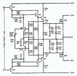
roender said:Hi,
I have tried a lot of output (BJT only) topologies, CFP, double and triple follower. After many listening days, the best in IMHO is the following:
I agree. I've been refining a version of this for 15 years. Originally saw it in the Ampzilla III, also years before in the Marantz 500. In the Ampzilla the the bases are pulled to the opposite rail. Very good low level detail, spooky at times.
Mike.
roender said:
Yes, at least at 15% output idle power
Hi Roender,
does this only apply to class A/B? Does it change for class A?
Regards
Harry
Torn Transients
Quote from KBK
Yeah! What he said!
Like I've said many a time before: I don't do the technical lingo. But I do know my stuff. Quite well, in fact.
Scopes don't measure reality. The merely report back a bunch of data that can be interpreted by a human. The resultant data is based on the test and what a scope does. Nothing more.
Some people can garner quite a bit from that data. Some do less well. some of what i speak of won't show up on a scope. But the ear hears it.See my post in the off topic area, on loudspeaker cables.
It concerns the human hearing mechanism,and an explanation why linearity to high sampling frequencies and/or inter-channel phase considerations are paramount.
****************************
As a circuit and product designer for over 30 years I try to be open minded and to learn from people who know more than me. I have never heard of a "Torn transient" and in searching the web for any other information I am coming up with nothing. Please KBK, educate me. If you do not have any technical information to study, how can your ears tell you that this is the etiology of the issue? Listen only to speakers, match devices, pronounce that a technical problem exists without anything? Where does the name "torn transients" come from?
Greg
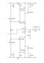
Guillermo,
Don't like it much.....
When the active side is passing heavy current, there is substantial voltage drop across the 0R22, and with fixed bias between the bases of the pre-drivers, the inactive side turns off. This is all predictable, standard Class AB fact.
This means the outputs MUST turn off, and the switch off of a CFP is fairly drawn out and messy because of the very high gain at the base/emitter junction of the output device.
The Vbe of the pre-driver is fairly constant because current through it does not much vary. The driver has the toughest time; its collector current varies from 0.6/47 + 1 (14mA) (the 1 here is the base bias for the output device) to around 1.8/47 + 75 (113mA), although the Vce works against us somewhat increasing the maximum current slightly. So 80% of the Vbe distortion is introduced through the output device only, the rest at the driver, and this is corrected by the negative feedback loop. BUT it is very tough to correct the spray of artefacts injected into the speaker at the point where the outputs turn off, this is the main problem, and transient instability at crossover is a likelihood too.
I like a CFP driver at high current, but a CFP output stage is problematic - in my opinion, and I'm only one guy, so don't take this as gospel.
Cheers,
Hugh
- Status
- Not open for further replies.
- Home
- Amplifiers
- Solid State
- Power Amplifier Output Topologies