jethari said:
Wasimbhai
You will have to disconnect the internal amplifier from the driver first. See if you can remove the driver and access the amplifier, do not attempt to dismantle the enclosure. Once you have access inside, disconnect the amplifier from the input terminals and from the driver. Once this is done, you can connect the NMOS output to the driver. Always remember, do not connect the output of one power amplifier to the input of another one, there's bound to be a lot of fireworks!!!
Hari
Hi
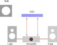
Oh!!!!!!!! misunderstanding !!! . My friend I have Nmos to run my two speakers (left and right) and I want to connect the sub woofer along with the speakers for more bass. the stereo signal I have from the DVD how can I convert them into mono and send them to my sub woofer. will that make sense? let me show you a diagram
Attachments
You will need to construct a low pass filter circuit and connect it between the DVD and the sub woofer. You will find one at the site I mentioned.
Gajanan Phadte
Gajanan Phadte
go and read the ESP site.
and
search for the filters threads.
You need a summing amplifier with a low pass filter and a PSU as a minimum.
and
search for the filters threads.
You need a summing amplifier with a low pass filter and a PSU as a minimum.
Hi All
Thanks a lot everybody. AndrewT has given me good direction. because I want left and right Chanel signals from DVD together for the sub woofer.
THANKS ALL
Regards
Thanks a lot everybody. AndrewT has given me good direction. because I want left and right Chanel signals from DVD together for the sub woofer.
THANKS ALL
Regards
Sub woofer filter is always fed with both L&R signals because ear cannot sense the direction of these low frequencies, the reason u find only one sub in a system.
Gajanan Phadte
Gajanan Phadte
Hi,
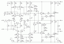
the output source resistors are in the drains.
VR2 is too small.
The two pole compensation may be difficult to debug.
the output source resistors are in the drains.
VR2 is too small.
The two pole compensation may be difficult to debug.
That's on purpose. It's really better that way. Helps to even half-waves. You know it's a quasicompl. topology, so they are not idealy even.AndrewT said:the output source resistors are in the drains.
I've simulated that schematics and VR2 should be aprox. 2 ohm for 70mA of otput stage current. Do you think it's a mistake?
So you have only simulated it?
In a real circuit with parts that have tolerances VR2 and the series resistor will need greater adjustment range. The series resistor needs to be reduced in value and the potentiometer increased in value.
Source resistors will be needed or else the FETs won't share current very well. They might need to be a bit larger than 0.1 ohm.
Very cool 2 pole miller, I've actually built the EF BJT versionBy Niroborn:What do you think about that kind of modification?
(father of Quasi) with this mod. I think the 2 cascodes are unnesessary as
the slight PSRR advantage and lower voltage across the LPT
do not justify all those added parts.(maybe 1 cascode if you ran
+-75V) On the CCS side of the LPT a red led with decoupling
cap is good enough.VD5 is a good idea that I actually use as well,
(just in case).
Also 2 pairs IRFP260 would indeed be "pushing it'
 for 2 ohms !
(4-5 pair recommended)
Yes, I've only simulated it yet, but I'm gonna solder it shortly.megajocke said:So you have only simulated it?
In a real circuit with parts that have tolerances VR2 and the series resistor will need greater adjustment range. The series resistor needs to be reduced in value and the potentiometer increased in value.
Source resistors will be needed or else the FETs won't share current very well. They might need to be a bit larger than 0.1 ohm.
It,s a good idea, I'll consider it.
I've tried to put source resistor, but there is a problem with simmetry of half waves that way. Can't explain in details - lack of technical english, you know.
ostripper said:
Very cool 2 pole miller, I've actually built the EF BJT version
(father of Quasi) with this mod. I think the 2 cascodes are unnesessary as
the slight PSRR advantage and lower voltage across the LPT
do not justify all those added parts.(maybe 1 cascode if you ran
+-75V) On the CCS side of the LPT a red led with decoupling
cap is good enough.VD5 is a good idea that I actually use as well,
(just in case).
Also 2 pairs IRFP260 would indeed be "pushing it'
(4-5 pair recommended)
Thanks for you presious comments, I'll consider them.
All that cascods and diod circuits they are slightly improving THD, bandwidth and very cheap, so I think why not. The THD on 20kHz sine wave <0.05% in 1MHz band at nominal power (300w 2 ohm). That's what simulation tells. What's in real life I can't tell yet.
In original NMOS amp I've used 2 pair of IRFP260N at even 1 ohm half year ago - they are still alive.
The "quasor" amp is very interesting (FET for Vbe and D.self
CCS with decoupling cap)
Strange using Baxandall Diode for fet as qausi does not in
the nmos but does in the BJT version "brother of quasi".
Is this a design by Dr. jagodic of serbia??
CCS with decoupling cap)
Strange using Baxandall Diode for fet as qausi does not in
the nmos but does in the BJT version "brother of quasi".
Is this a design by Dr. jagodic of serbia??
You're right, there is no need for that diode here. That's only sufficient when the OP devices are BJT.
Anyway the schema has more design mistakes... I wouldn't recommend to build it.
Anyway the schema has more design mistakes... I wouldn't recommend to build it.
Ferencz, what are your opinions on the "quasi" line of amps ?
(Design flaws/changes/improvements)
I am testing a universal "blameless" design and left the board
open to any design change.
The one I am experimenting on now is a EF "non-Qausi"
using BJT's , (sort of a "father of quasi"). 😀
(Design flaws/changes/improvements)
I am testing a universal "blameless" design and left the board
open to any design change.
The one I am experimenting on now is a EF "non-Qausi"
using BJT's , (sort of a "father of quasi"). 😀
!
Well ferencz I must tell you that your words are not correct.One guy "mrrocky" has already built Quasor amplifier with succes.I will try too translate his words...
Legend Quasor is finished,it sounds very good,DC voltage on speaker is 8mV and sound is better than Legend Stage Master witch I also built.Hi tested also Zeck PT-5(500W at 4ohm) amplifier and after listening we have confirmed that QUASOR was better(sound) than the Zeck at least 2 times and also it's more powerfull than Zeck.
Why you don't recommend quasor???
ferencz said:You're right, there is no need for that diode here. That's only sufficient when the OP devices are BJT.
Anyway the schema has more design mistakes... I wouldn't recommend to build it.
Well ferencz I must tell you that your words are not correct.One guy "mrrocky" has already built Quasor amplifier with succes.I will try too translate his words...
Legend Quasor is finished,it sounds very good,DC voltage on speaker is 8mV and sound is better than Legend Stage Master witch I also built.Hi tested also Zeck PT-5(500W at 4ohm) amplifier and after listening we have confirmed that QUASOR was better(sound) than the Zeck at least 2 times and also it's more powerfull than Zeck.
An externally hosted image should be here but it was not working when we last tested it.
An externally hosted image should be here but it was not working when we last tested it.
An externally hosted image should be here but it was not working when we last tested it.
An externally hosted image should be here but it was not working when we last tested it.
Why you don't recommend quasor???

- Home
- Amplifiers
- Solid State
- Power amp under development