Re: Hi again !
I am, just getting ready for bed. It's just after midnight and I'm beat.
Ciao
Q
zeonrider said:I see you is online now !
Regards zeoN_Rider
I am, just getting ready for bed. It's just after midnight and I'm beat.
Ciao
Q
Thanks Quasi and Keypunch!
Hello,
Yes I thought, my question would be one of the most frequently asked ones. I even followed the thread until page 30 (or so) when it was new, but then i lost track. I did not knew, if there were any new developments (100 pages...?).
Thank you very much Keypunch, for your link (very good idea) -collection. This will help alot of people. First thing I did was to save the link to this threadpage.
One problem of the search engine on diyaudio is that one is not able to search only one thread. Not very useful in my case.
Quasi:
The small layout looks perfect! The size is perfect too! The AMP could be placed on standard 100x75mm boards (I like it when pcb-boards fit to standard pre-cutted boards) or a stereo version on 100x160mm.
The AL-Bracket is a genius Idea, just as your part arrangement. Everything on one heatsink, easy too mount.
I am looking forward to build this small version of the NMOS Amplifier. I happen to have a suitable Torroid with 2x35VAC secondary. You don't have to hurry with the schematic and the tracks. I still have to build a Symasym.
Greetings
Black
Re[02]: Thanks Quasi and Keypunch!
Your welcome Black. One of my ToDos that will take some time is build a document with all the important information collected in it and organized in related topics, maybe indexed. I started the document actually, but a software bugs forced me to put it on hold. The bugs are addressed for most part, but I have had a number of personal matters middle of last year and again the latter half of this year keeping me off the thread as well for most part. Maybe in a couple months I can resume the effort which I suspect will take about 6 months to complete with the growth of the thread.
It has been often commented that the diyAudio search engine is not effective as expected. This is in part the search engine, but also because the information one is looking for may not be using the words expected, or the poster may have mistyped the word, used a short form or ordered the words differently than you expect that is important in your seach and at times happens to be the posting that is of greatest interest that will then be missed as result. Fact is this will happen using any of the popular search engines like Yahoo, Google, et al as this is not a search engine issue. It is just a fact of humans and the different ways things can be expressed.
You can actually search just a thread, there is the "Search this Thread:" at the bottom of each page of the thread to the right. This thread search function is a simple search compared to the diyAudio search page. So have suggesged on diyAudio to use a Google or Yahoo to seach using diyAudio as a criteria. Using this approach some have suggested they have had better success than the diyAudio seach facility.
Black,
Are you aware the Symamp is very part dependant which makes it difficult to use alternate parts and the setup of the Sysamp is also a bit more challenged to setup as result? For example the effort and changes to work with the 2SC5200/2SA1943 output devices. Maybe you would want to consider the "Brother of Quasi" if you want a BiPolar.
The current downside if the BoQ is the PCB is designed for TO-3 devices as that was the overwhelming requested, not plastic TO-247 like BiPolar devices. I think it would not be too hard to tweak the BoQ PCB to work with plastic BiPolar devices if you have a bit of patience using a graphics editing program. Case in point is the 1, 2, and 4 pair version of the quasi MOSFET I have created as well as the many tweaks and in some cases major (in time) modifications I have made to the MOSFET boards to suit my personal needs be it a part size difference or adding in option for a different feedback network.
Quasi has come out with the TO-220 MOSFET version and made it compact (the base design is actually compact as well as most of space is for the physical space of the output devices) again due to may requests. I also want to build a TO-220 version, but after some thought decided I do so using the original base design some months ago as I think the base design has endearing qualities I felt important to me.
Regards,
John L. Males
Willowdale, Ontario
Canada
11 January 2007 13:52
11 January 2007 14:17 Typo correction
11 January 2007 14:21 Typo correction
BlacK_Chicken said:Thank you very much Keypunch, for your link (very good idea) -collection. This will help alot of people. First thing I did was to save the link to this threadpage.
One problem of the search engine on diyaudio is that one is not able to search only one thread. Not very useful in my case.
Your welcome Black. One of my ToDos that will take some time is build a document with all the important information collected in it and organized in related topics, maybe indexed. I started the document actually, but a software bugs forced me to put it on hold. The bugs are addressed for most part, but I have had a number of personal matters middle of last year and again the latter half of this year keeping me off the thread as well for most part. Maybe in a couple months I can resume the effort which I suspect will take about 6 months to complete with the growth of the thread.
It has been often commented that the diyAudio search engine is not effective as expected. This is in part the search engine, but also because the information one is looking for may not be using the words expected, or the poster may have mistyped the word, used a short form or ordered the words differently than you expect that is important in your seach and at times happens to be the posting that is of greatest interest that will then be missed as result. Fact is this will happen using any of the popular search engines like Yahoo, Google, et al as this is not a search engine issue. It is just a fact of humans and the different ways things can be expressed.
You can actually search just a thread, there is the "Search this Thread:" at the bottom of each page of the thread to the right. This thread search function is a simple search compared to the diyAudio search page. So have suggesged on diyAudio to use a Google or Yahoo to seach using diyAudio as a criteria. Using this approach some have suggested they have had better success than the diyAudio seach facility.
Quasi:
I am looking forward to build this small version of the NMOS Amplifier. I happen to have a suitable Torroid with 2x35VAC secondary. You don't have to hurry with the schematic and the tracks. I still have to build a Symasym.
Greetings
Black
Black,
Are you aware the Symamp is very part dependant which makes it difficult to use alternate parts and the setup of the Sysamp is also a bit more challenged to setup as result? For example the effort and changes to work with the 2SC5200/2SA1943 output devices. Maybe you would want to consider the "Brother of Quasi" if you want a BiPolar.
The current downside if the BoQ is the PCB is designed for TO-3 devices as that was the overwhelming requested, not plastic TO-247 like BiPolar devices. I think it would not be too hard to tweak the BoQ PCB to work with plastic BiPolar devices if you have a bit of patience using a graphics editing program. Case in point is the 1, 2, and 4 pair version of the quasi MOSFET I have created as well as the many tweaks and in some cases major (in time) modifications I have made to the MOSFET boards to suit my personal needs be it a part size difference or adding in option for a different feedback network.
Quasi has come out with the TO-220 MOSFET version and made it compact (the base design is actually compact as well as most of space is for the physical space of the output devices) again due to may requests. I also want to build a TO-220 version, but after some thought decided I do so using the original base design some months ago as I think the base design has endearing qualities I felt important to me.
Regards,
John L. Males
Willowdale, Ontario
Canada
11 January 2007 13:52
11 January 2007 14:17 Typo correction
11 January 2007 14:21 Typo correction
Re: Mini - Quasi
The traces on T9 and T10 look odd. I need to look closer.
Shawn.
quasi said:Here's the mini board. Could be used for multi-channel amplifiers, but also compact stereo units. Has been designed for rails up to +/- 55v (FET dependant).
Cheers
Q
The traces on T9 and T10 look odd. I need to look closer.
Shawn.
Re[02]: Mini - Quasi
Quasi,
Very nice base design for the mini.
I am curious what you use as criteria to the different dimensioning of the module PSU rail electrolytic filter capacitors? The base design uses 330uF, the high power uses 470uF and the mini uses 100uF.
Are you aware there seems to be alot of dead copper areas not connected to anything on the mini version of the PCB? My guess is the PCB software had some sort of setting related to fill or ground plane? I am not sure, just that I can see alot of distracting copper areas.
I am curious about T6/T7 and T9/T10 on the mini board. They are not mounted to one common heatsink like the original board. I am assuming T6/T7 produce less heat than T9/T10 hence the latter on the main heatsink. I wanted to know how the different thermal coupling of T6/T7/T9/T10 in this PCB design vs the base design may cause due to the thermal coupling differences in the module behaviour?
Regards,
John L. Males
Willowdale, Ontario
Canada
11 January 2007 14:10
11 January 2007 14:16 Typo correction
Re: Re[02]: Mini - Quasi
Why waste your etching solution stripping the entire board? Also the more copper you strip, the longer it takes. A few posts back (on the other thread) I think Q made a comment that he was making an effort to process more efficiently. I could be wrong?
Shawn.
keypunch said:Quasi,
Are you aware there seems to be alot of dead copper areas no connected to anything on the mini version of the PCB?
Regards,
John L. Males
Willowdale, Ontario
Canada
11 January 2007 14:10
Why waste your etching solution stripping the entire board? Also the more copper you strip, the longer it takes. A few posts back (on the other thread) I think Q made a comment that he was making an effort to process more efficiently. I could be wrong?
Shawn.
Re: Re: Re[02]: Mini - Quasi
Isolated copper not only looks ugly, it can cause parasitic capacitance problems. 😉
TomWaits said:Why waste your etching solution stripping the entire board? Also the more copper you strip, the longer it takes.
Isolated copper not only looks ugly, it can cause parasitic capacitance problems. 😉
Re[04]: Mini - Quasi
Hi Shawn,
Understand about saving time and etching solution, but I think if you look closely at board, it seems the PCB CAD software has gone about this in very odd fashion and leaves some really distracting areas and questionable artifacts. Examples include the odd very thin traces under the module PSU filter capacitors that extend to the 0.1uF capacitors, the thick traces under/near the module PSU filter capacitors and not connected to the thin trace area under the same capacitors, under VR2, the spots between the leads of the output MOSFET devices, etc. Also it seems the PCB CAD software is not showing the outside board border as the fill extends more than one sees of traces on the sides of the board.
Regards,
John L. Males
Willowdale, Ontario
Canada
11 January 2007 14:33
11 January 2007 14:46 Typo correction
11 January 2007 15:02 Typo correction
Re[06]: Mini - Quasi
Al,
If one had one contigious copper area and only connected to signal, or should it be earth, gound would that elimiate the parasitic capacitance?
Is same parasitic capacitance issue true if one uses the component side to be all copper except with no copper about the holes for the components? I assume in this case should be single point grounded as well and would be signal or earth ground?
Regards,
John L. Males
Willowdale, Ontario
Canada
11 January 2007 14:44
11 Janaury 2007 14:50 Typo corrections
11 January 2007 14:54 Typo correction
Re: Re: Re: Re[02]: Mini - Quasi
Better to fatten VCC_+ and larger GND area? Better still to shrink the design as much as possible to avoid filler? Yes, isolated copper is not wanted. Mouse boards are very nice. 🙂
Shawn.
pinkmouse said:
Isolated copper not only looks ugly, it can cause parasitic capacitance problems. 😉
Better to fatten VCC_+ and larger GND area? Better still to shrink the design as much as possible to avoid filler? Yes, isolated copper is not wanted. Mouse boards are very nice. 🙂
Shawn.
Re[08]: Mini - Quasi
Shawn,
I think the board is compact enough and I would favour leaving the trace spacing as is without the filler. I would think parasitic capacitance is still a factor if the traces are too close to each other for audio purposes. Digital applications can tolerate closer traces as their signals are generally logic based and have a greater tolerance for capacitance than an audio signal.
Regards,
John L. Males
Willowdale, Ontario
Canada
11 January 2007 15:44
TomWaits said:
Better to fatten VCC_+ and larger GND area? Better still to shrink the design as much as possible to avoid filler? Yes, isolated copper is not wanted. Mouse boards are very nice. 🙂
Shawn.
Shawn,
I think the board is compact enough and I would favour leaving the trace spacing as is without the filler. I would think parasitic capacitance is still a factor if the traces are too close to each other for audio purposes. Digital applications can tolerate closer traces as their signals are generally logic based and have a greater tolerance for capacitance than an audio signal.
Regards,
John L. Males
Willowdale, Ontario
Canada
11 January 2007 15:44
Hello Keypunch,
I am building the symasym at the moment, therefore I am not able to build another amp. But I plan to build the to-220 Version one day.
Greets
Black
I am building the symasym at the moment, therefore I am not able to build another amp. But I plan to build the to-220 Version one day.
Greets
Black
Re: Re[08]: Mini - Quasi
 Shawn.
keypunch said:I would think parasitic capacitance is still a factor if the traces are too close to each other for audio purposes. Digital applications can tolerate closer traces as their signals are generally logic based and have a greater tolerance for capacitance than an audio signal.
Regards,
John L. Males
Willowdale, Ontario
Canada
11 January 2007 15:44
Shawn.Hi Quasi !
for:
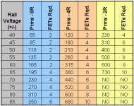
10 FETS - 85V - 8 Ohm = ___RMS??
what is the delivered power ???
regards
(sorry for my poor english !)

for:
10 FETS - 85V - 8 Ohm = ___RMS??
what is the delivered power ???
regards
(sorry for my poor english !)
Re: Re: Re: Re[02]: Mini - Quasi
Re: Filtering capacitors. It's all about space available on the board and diminishing returns. If you can get a larger value capacitor to fit then by all means put it in. Much larger value capacitors can be found for rails under 50v.
T6 & T7 will dissipate just over 0.5 watt each with rails of 50v. They do not need to be thermally coupled because they actually perform different functions. But it's easy to use the same heatsink. T9 & T10 perform the same function by driving into the 220 ohm resistor creating the voltage drive for the output FETs. These will dissipate around 0.8 watts each at idle and need to be heatsinked too. They mount on the main bracket because of their proximity to the output devices. Being on the same bracket should keep their temperatures the same and this has some importance with regard to thermal stability once the bias is set. On the other larger module it was too difficult to mount them in this fashion and in practice did not seem to matter as the thermal stability is excellent.
Ugly ??? Arrgh them bells .... I doubt there will be much stray capacitance issues with this layout. The impedances throughout the cct are quite low. The area of doubt in my mind is the copper layer under the FETs, but these are "shielded" by the aluminium bracket that is grounded via the heatsink. In any case the major unconnected copper islands can be linked by straps to the "noisy" ground. Finally I'll post a "clean" and "more attractive" board tonight as an alternative.
Cheers
Q
keypunch said:Quasi,
I am curious what you use as criteria to the different dimensioning of the module PSU rail electrolytic filter capacitors? The base design uses 330uF, the high power uses 470uF and the mini uses 100uF.
I am curious about T6/T7 and T9/T10 on the mini board. They are not mounted to one common heatsink like the original board. I am assuming T6/T7 produce less heat than T9/T10 hence the latter on the main heatsink. I wanted to know how the different thermal coupling of T6/T7/T9/T10 in this PCB design vs the base design may cause due to the thermal coupling differences in the module behaviour?
Re: Filtering capacitors. It's all about space available on the board and diminishing returns. If you can get a larger value capacitor to fit then by all means put it in. Much larger value capacitors can be found for rails under 50v.
T6 & T7 will dissipate just over 0.5 watt each with rails of 50v. They do not need to be thermally coupled because they actually perform different functions. But it's easy to use the same heatsink. T9 & T10 perform the same function by driving into the 220 ohm resistor creating the voltage drive for the output FETs. These will dissipate around 0.8 watts each at idle and need to be heatsinked too. They mount on the main bracket because of their proximity to the output devices. Being on the same bracket should keep their temperatures the same and this has some importance with regard to thermal stability once the bias is set. On the other larger module it was too difficult to mount them in this fashion and in practice did not seem to matter as the thermal stability is excellent.
pinkmouse said:
Isolated copper not only looks ugly, it can cause parasitic capacitance problems. 😉
Ugly ??? Arrgh them bells .... I doubt there will be much stray capacitance issues with this layout. The impedances throughout the cct are quite low. The area of doubt in my mind is the copper layer under the FETs, but these are "shielded" by the aluminium bracket that is grounded via the heatsink. In any case the major unconnected copper islands can be linked by straps to the "noisy" ground. Finally I'll post a "clean" and "more attractive" board tonight as an alternative.
Cheers
Q
Re: Re: Re: Re: Re[02]: Mini - Quasi
Thank you! 🙂
Sorry, but you know they really do! 😉
TomWaits said:Mouse boards are very nice. 🙂
Thank you! 🙂
quasi said:Ugly ??? Arrgh them bells ....
Sorry, but you know they really do! 😉
Re: Re: Re: Re: Re: Re[02]: Mini - Quasi
I know they do, particularly in very sensitive circuits. Indeed PCB techniques are employed to conteract or protect senstive stages. All I am saying is (is give peace a chance?) in this application it won't matter. But I'll build one and confirm or report otherwise.
Cheers
Q
pinkmouse said:Sorry, but you know they really do! 😉
I know they do, particularly in very sensitive circuits. Indeed PCB techniques are employed to conteract or protect senstive stages. All I am saying is (is give peace a chance?) in this application it won't matter. But I'll build one and confirm or report otherwise.
Cheers
Q
Re: Re: Re: Re: Re: Re: Re[02]: Mini - Quasi
Of course!
I was actually mostly talking about the aesthetics mostly anyway. I just can't stand isolated copper. I hate it almost as much as I do curved tracks! 😀
quasi said:...is give peace a chance?
Of course!
I was actually mostly talking about the aesthetics mostly anyway. I just can't stand isolated copper. I hate it almost as much as I do curved tracks! 😀
- Home
- Amplifiers
- Solid State
- Power amp under development