I'm just curious...
To what MOSFETs are you comparing those IGBTs?
What rise/fall times or waveforms are you getting from the MOSFETs?
My experience is the opposite since replacing two IRFP460 [from ST] by two SKP10N60 [from Infineon] reduced total losses somewhat in a single-phase 160-240V AC to 450V DC 2000W PFC simple home-made prototype, specially at full load, and ugly 10-30Mhz RF ringing was no longer present at switching transients
PD: I'm using a coupled inductor plus saturable reactor combination to delay the current rise about 100nS [giving the switches enough time to saturate] and then ramp-up the current on the switches at 50A/us in order to avoid dissipation during diode reverse recovery [stored energy on this inductor is dumped back to the output at turn-off and next cycle is delayed if it starts when the inductor is still discharging]. This method reduces dramatically switching losses but the 'saturable core' quickly overheats since I actually have no access to saturable reactor cores and I'm using standard ferrite materials with high losses for that purpose
Hi,
well...I have the dc offset solved.... how does -40mV sound? nnnnnnot bad I think, part of the problem actually was pspice..Otherwise I would have found it much sooner.
Curiously the PWM output still has what looks like supply pumping that hasnt' changed much at all. Should I care?
I find my highest levels of distortion with this circuit occur with low inputs.. 1W output for instance is the worst...while 500Watts out has the last distortion. Is that spice playing a game with me?
Chris
Hi Chris!
Don't simulate, build it! 🙂
I built it yesterday (same principle, but different realising), and it work perfectly! Author is right: it's the ultimate (SE) classD!
"the PWM output still has what looks like supply pumping"
What do you mean?
Thank you for the link again!
Don't simulate, build it! 🙂
I built it yesterday (same principle, but different realising), and it work perfectly! Author is right: it's the ultimate (SE) classD!
"the PWM output still has what looks like supply pumping"
What do you mean?
Thank you for the link again!
Curiously the PWM output still has what looks like supply pumping that hasnt' changed much at all. Should I care?
How much ?`
Regards
Charles
How can be seen supply pumping on output?
I was wondering about this also at first. Then I came to the conclusion that he may be talking about the PWM signal as such, i.e. BEFORE the output filter.
There you will see it of course, simply because you switch between the two rails.
Regards
Charles
Hi,
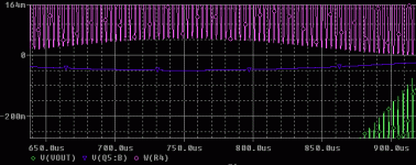
Yes, I have about a 1 volt of ripple on the pwm output, which is the inverse of the input signal and carries through out the system.
The DC offset would cause the ripple to be far worse on alternate wave peaks and also affect the output voltage. With the dc offset minimally optimised it carries through just over a 1/4 volt.
Pafi, If I built it i'd be having +-200amps cross conduction right now. What was your implementation of the mosfet driver?
Chris
Yes, I have about a 1 volt of ripple on the pwm output, which is the inverse of the input signal and carries through out the system.
Don't forget the forward voltage of the "freewheeling diodes".
Regards
Charles
Hey eva, you should have a play with a Fairchild IRFP460A. We use then at work very often. Unbelievable performance for a bread-and-butter mosfet. They also claim a turnoff time of 6nS.Eva said:I've got performances as good as 50ns or less charge/discharge times for an IRFP460 switching 300V [including 'miller' capacitance effects, very noticeable at these high voltages]

Hi, Chris!
"Yes, I have about a 1 volt of ripple on the pwm output, which is the inverse of the input signal and carries through out the system."
Yes, it indicates the natural "pumping". The current converted to voltage on Rds.
"The DC offset would cause the ripple to be far worse on alternate wave peaks and also affect the output voltage. With the dc offset minimally optimised it carries through just over a 1/4 volt."
I don't understand this.
"Pafi, If I built it i'd be having +-200amps cross conduction right now. What was your implementation of the mosfet driver?
Chris"
IR2110. BTW: I use IGBTs because supply voltage is over +/-100V.
To avoid cross-conduction, slow down gate charging.
Hi Pafi,
Well with bad DC offset the output power would look uneven, 600watt peak....200 watt peak......600........200....etc
Yeh, I figured out what needs to be done to fix it (cross conduction) but instead of doing that I'm working on a different driver circuit altogether for it.
Regards,
Chris
Well with bad DC offset the output power would look uneven, 600watt peak....200 watt peak......600........200....etc
Yeh, I figured out what needs to be done to fix it (cross conduction) but instead of doing that I'm working on a different driver circuit altogether for it.
Regards,
Chris
- Status
- Not open for further replies.
- Home
- Amplifiers
- Class D
- poor switching