I principal, there is three different designs for n-channel mos-fet power amplifier that I have come across so far. I like to keep it simple and believe a good performing amplifier don't have to be complicated. Inspired by Pass MF-12, Holton N-channel and others, I think it would be fun to design and build one myself, but which one? Target output fets are IRFP520.
I would appreciate comments or experience from any of these designs. Sound, general performance, stability is of course of interest. And of course, how do they compare?
I would appreciate comments or experience from any of these designs. Sound, general performance, stability is of course of interest. And of course, how do they compare?
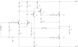
Design A
Design A uses a double differential and is perhaps the most symmetrical of all designs. The second stage (Q1, Q2) don't have to be differential, a conventional CE works fine.
This design have been the hardest of the three to perform well in simulation.
Pros: Symmetrical, uses a real differential amplification.
Cons: ?
Attachments
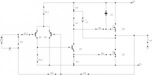
Design B
Design B uses a single transisitor for phase shift. All amplification is in the input stage (Q4), Q3 usally has a gain of one but can be more. It is simple, simulates good and is a proven design.
Holton N-channel is a working example of this design!
Pros: Simple, proven.
Cons: ?
Design B uses a single transisitor for phase shift. All amplification is in the input stage (Q4), Q3 usally has a gain of one but can be more. It is simple, simulates good and is a proven design.
Holton N-channel is a working example of this design!
Pros: Simple, proven.
Cons: ?
Attachments
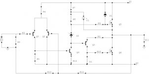
Design C
This design I think is the most classical one, a two stage amplifier (Q3, Q4), with phase shift (Q1), and voltage feedback (Q2). It has been proven over many years and works well.
Pass MF-12 is an example of this design.
Pros: Simple, classical.
Cons: ?
This design I think is the most classical one, a two stage amplifier (Q3, Q4), with phase shift (Q1), and voltage feedback (Q2). It has been proven over many years and works well.
Pass MF-12 is an example of this design.
Pros: Simple, classical.
Cons: ?
Attachments
If "simple" is in your shopping list, nothing beats true single ended operation against a current source. Of course this halfs the efficency, but something can be regained when using bootstrap to achieve rail to rail output operation.
Look at this example circuit (think MOSFETs instead of IBGTs):
http://www.linearaudio.de/scratch/IGBT-3.pdf
Regards,
Peter Jacobi
Look at this example circuit (think MOSFETs instead of IBGTs):
http://www.linearaudio.de/scratch/IGBT-3.pdf
Regards,
Peter Jacobi
Essentially by adjusting current through the first gain stage, or in design C with a discrete and adjustable zener. Anyway, there must be some temprature compensation.Tube_Dude said:How you adjust the bias of the output mos-fets? 😉
pjacobi said:If "simple" is in your shopping list, nothing beats true single ended operation against a current source. Of course this halfs the efficency, but something can be regained when using bootstrap to achieve rail to rail output operation.
...
I don't agree the complexity is an issue of class A or AB. The complexity and component count of your proposal is very much the same as in design C, and design B is simpler. Nice with CFB though! What do you think is the audible difference between VFB and CFB from your experience?
By the way, fet's are IRFP260N: Vdss=200V; Rdson=0.04ohm; Id=50A; Pd=300W. Nasty!

bjornagain said:I don't agree the complexity is an issue of class A or AB. The complexity and component count of your proposal is very much the same as in design C, and design B is simpler. Nice with CFB though! What do you think is the audible difference between VFB and CFB from your experience?
That was overlap at posting. When I did my posting I haven't seen your simpler designs B and C yet.
CFB issues (Hey, where is the CFB police? Strictly, speaking this isvoltage sensed feedback into a low impedance node):
I can't do my day job, post on this forum and actually build these amps. Anyway, I'm waiting for more cheap grabs at Ebay, before my first prototype will be done. So I can't tell you of subjective differences.
It's more philisophical, Occams Razor as applied to amplifier design. Why the heck buffer the feedback signal with a follower when it has a source impedance of milliohms?
Regards,
Peter Jacobi
Comments/Questions...
Design A: The collectors of Q1/Q2 go to different rail voltages. This should make it very hard/impossible to find resistor values that balance the currents and gains... does it work?
Design B: I don't think Q3 can be set for more than unity gain because it's also a phase splitter. If you add gain, it will only be added to the inverted phase.
Design C: Mosfet-12, I want to build one of these, I got some IRPF450s cheap...
It seems like to me that all these designs are considered 3-stage amps instead of 2-stage.
Design A vs Design C, I would suggest Design C. Same number of transistors. It's not as symmetrical but you will win on HF response.
You can add my design to your list as well:
http://www.diyaudio.com/forums/showthread.php?s=&threadid=14320
Regards
x-pro
http://www.diyaudio.com/forums/showthread.php?s=&threadid=14320
Regards
x-pro
I see what you mean, the main (or perhaps only) purpose of the buffer transistor must be to compensate for the Vbe of the input transistor in order to get a descent low offset. Besides, this buffer must introduce some problems by nature, it doesn't improve the signal in anyway. I have tried this coupling with jfet and bjt mixed and it works well (besides the offset). Some describe this as a long tailed pair, which I think is not correct.pjacobi said:...
CFB issues (Hey, where is the CFB police? Strictly, speaking this isvoltage sensed feedback into a low impedance node):
...
Why the heck buffer the feedback signal with a follower when it has a source impedance of milliohms?
...
One definition of a CFB is a high impedance input and a low impedance feedback input, like your circuit. The feedback net does have some impedance, don't you think?
It probably works, it works in the simulator but doesn't shine. I have two schemas I can post if you want.azira said:...
Design A: ... does it work?
...
Design C: Mosfet-12, I want to build one of these, I got some IRPF450s cheap
...
It seems like to me that all these designs are considered 3-stage amps instead of 2-stage.
...
Design A vs Design C, I would suggest Design C. Same number of transistors. It's not as symmetrical but you will win on HF response.
I really like MF-12 too!
Why better HF response?
Thanks, very nice! A practical implementation of design B 🙂x-pro said:You can add my design to your list as well:
http://www.diyaudio.com/forums/showthread.php?s=&threadid=14320
...
x-pro said:You can add my design to your list as well:
http://www.diyaudio.com/forums/showthread.php?s=&threadid=14320
...
Ooops! It's not like B at all: Q1 is a P-channel and the stage is non inverting. Very interesting!
Hi Bjornagain,
Nice thread going on here, difficult dissicion? Let me put in my 2 cents:
Design B:
I have had quite some experience with that output last 2 months and liked it very much, very much indeed. I have had a long discussion on that output stage on the JLH-10W Class A thread. You might wanna look into that one, but I warn you (hi hi hi ) It's not everybodies cuyp of thee.. (hi hi hi) ..It simulated great and measured accordingly: supurb.. BTW the amplifier is considdered a 2-stage amplifier by at least 3 notable HiFi audio autheurs and I tend to agree... Judging from my experience with this output stage, X-pro's schematic should work very well too, if not better ..
Design C:
Considdering that a well desiged amplifier lineairity is domminated by the output stage lineairuty, this design might not be a good chooise ... This output stage is famous for it nonlinearity (BTW same three autheurs), and I also suspect some HF issues, but maybe I'm just being pessimitic now....It's non-symmetric, not ellegant, plain ugly to me actually..
Design A: My chooise (how do you spell that ? choiche? choise, chooishe?? ).. It's new to me.. nice original idea... offcourse some source resistors ertc etc.. but you know that.. the topology is very appealing to me ...I don't expect much problems with the different colector voltages.. and it can be solved by design.. cascode or something like that...could be very interesting.. I might just buy a couple of IRF540 for an Euro or so and build one myself... come on be adventurous.. build 'A' !
If Class A is your goal, you don't have to worrie about Iq adjustment, a few source resistors will make it easy adjustable and quite stable...
PS
hi hi.. how about this:
voltage feedback works by controlling a voltage at a input trasistor, while current feedback works by regulating the current through the input resistor..?
Nice thread going on here, difficult dissicion? Let me put in my 2 cents:
Design B:
I have had quite some experience with that output last 2 months and liked it very much, very much indeed. I have had a long discussion on that output stage on the JLH-10W Class A thread. You might wanna look into that one, but I warn you (hi hi hi ) It's not everybodies cuyp of thee.. (hi hi hi) ..It simulated great and measured accordingly: supurb.. BTW the amplifier is considdered a 2-stage amplifier by at least 3 notable HiFi audio autheurs and I tend to agree... Judging from my experience with this output stage, X-pro's schematic should work very well too, if not better ..
Design C:
Considdering that a well desiged amplifier lineairity is domminated by the output stage lineairuty, this design might not be a good chooise ... This output stage is famous for it nonlinearity (BTW same three autheurs), and I also suspect some HF issues, but maybe I'm just being pessimitic now....It's non-symmetric, not ellegant, plain ugly to me actually..
Design A: My chooise (how do you spell that ? choiche? choise, chooishe??
).. It's new to me.. nice original idea... offcourse some source resistors ertc etc.. but you know that.. the topology is very appealing to me ...I don't expect much problems with the different colector voltages.. and it can be solved by design.. cascode or something like that...could be very interesting.. I might just buy a couple of IRF540 for an Euro or so and build one myself... come on be adventurous.. build 'A' !If Class A is your goal, you don't have to worrie about Iq adjustment, a few source resistors will make it easy adjustable and quite stable...
PS
hi hi.. how about this:
voltage feedback works by controlling a voltage at a input trasistor, while current feedback works by regulating the current through the input resistor..?
Hi again,
after some experimenting in Virtual Reality, I realized that design A has some efficientcy issues.. the possitive going signals clip a bit mpore below the +V rail.. that's not a big deal but still.. it is however the most linear of your 3 designs.. But I still think I would go with design B now ... better efficientcy and still very good linearity, more stable too ...
Regards,
Thijs
bjornagain said:
Why better HF response?
The design you showed and the MF-12 both have one leg of the input pair connected to the rail instead of a resistor. This has better HF response than a standard differential although it becomes a single ended application because the Miller effect on the strapped transistor goes away.
Ok, guess it's time for me to own up to my mistakes...
I looked at it again, I agree, the phase splitter isn't really a gain stage.
I looked at it again. I should have split up Q1/Q2 as seperate CEs and it would have been obvious that it'll work, my mistake for the "will it work comment".
Actually, I just realized it's a lot like an amp that I'm working on right now as well. I was trying to do it two-staged with AC coupling to the output FETS (before you start, it's not the worst audio thing I've done, my Zen has FANS on the heatsink, take THAT!) but I can't get it to work well. I would be interested in seeing your schemas if you can post them.
he amplifier is considdered a 2-stage amplifier by at least 3 notable HiFi audio autheurs and I tend to agree
I looked at it again, I agree, the phase splitter isn't really a gain stage.
It probably works, it works in the simulator but doesn't shine. I have two schemas I can post if you want.
I looked at it again. I should have split up Q1/Q2 as seperate CEs and it would have been obvious that it'll work, my mistake for the "will it work comment".
Actually, I just realized it's a lot like an amp that I'm working on right now as well. I was trying to do it two-staged with AC coupling to the output FETS (before you start, it's not the worst audio thing I've done, my Zen has FANS on the heatsink, take THAT!) but I can't get it to work well. I would be interested in seeing your schemas if you can post them.
azira said:I looked at it again, I agree, the phase splitter isn't really a gain stage.
it can be made to have (uneven) gains for the upper and lower output transistors, and most likely it does because of the bootstrap network. You can also disable the bootstrap and use just a single resistor for the upper end if you are concerned about uneven gains.
Design B is essentially a mosfet version of JLH with differential input stage. The 'current feedback" setup of JLH with a single transistor may just work better.
Hi Thijs,
thanks for your reply. Yes I also prefer design B, and I also think X-pro has an elegant solution for biasing, but it requires a two stage input stage, or a input capicator (which perhaps isn't a bad thing).
I had the same problems with design A to get a descent swing (and stability). And like Azira proposes, it works better with two CE in the second stage, and also emitter resisitors in the first stage. Too bad it doesn't work better!
Perhaps I should leave this topic about VFB and CFB in peace, I can sense a lot of emotions in the community...
thanks for your reply. Yes I also prefer design B, and I also think X-pro has an elegant solution for biasing, but it requires a two stage input stage, or a input capicator (which perhaps isn't a bad thing).
I had the same problems with design A to get a descent swing (and stability). And like Azira proposes, it works better with two CE in the second stage, and also emitter resisitors in the first stage. Too bad it doesn't work better!
Hmm, I think there is a difference - a low impedance input of a transistor (ideally 0 ohm) can't develop any voltage, so it's current controlled, and then it doesn't matter if there is a resistor in parallel with this input.tschrama said:...
hi hi.. how about this:
voltage feedback works by controlling a voltage at a input trasistor, while current feedback works by regulating the current through the input resistor..?
Perhaps I should leave this topic about VFB and CFB in peace, I can sense a lot of emotions in the community...
It seems to work equally fine in simulation with even or uneven gain, no big differencies. But I wonder how it sounds?millwood said:it can be made to have (uneven) gains for the upper and lower output transistors, and most likely it does because of the bootstrap network. You can also disable the bootstrap and use just a single resistor for the upper end if you are concerned about uneven gains.
...
He, he - It's nice to be human, isn't it!azira said:Ok, guess it's time for me to own up to my mistakes...
Agree, it works better. The I got this funny idea to bootstrap the emitters to get more swing. The schemas is for class A I think, I will post them later for you.I looked at it again. I should have split up Q1/Q2 as seperate CEs and it would have been obvious that it'll work, my mistake for the "will it work comment".
- Status
- Not open for further replies.
- Home
- Amplifiers
- Solid State
- Please rate designs for n-ch mosfet amp