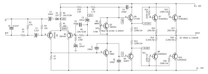
Hi there, Please provide a solution to the issue. I know very little about amplifiers. I purchased an amplifier board a few days ago and tried to sketch the circuit diagram. Both the original and the suggested diagrams are attached.
Regards -- opu
Regards -- opu
Attachments
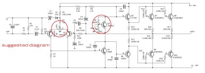
R3 / R6
just make same value 22k
R7 is little high
make 680 or 820 ohm
R9 / R10
make same value 3.3k
R9/R10 and R5/R4
are current sources
simple resistor values are set
to be correct current at 40 volt rails
long as your testing amp around 35 to 40
volts. If test voltage is much lower
current sources be off a little
and cause DC offset.
lowering R7 should help
most the problem.
Hi opusadat
As WhiteDragon said, some other things I also added.
R3 & R6 must be equal.
Q1 & Q2 needs to be a matched pair and thermally coupled.
C2 & D1 are drawn wrong, Anode of D1 connects to ground & C2+ connects to Cathode of D1.
By adding VR1 this will adjust the DC offset, however it also changes the GAIN BANDWITCH of the input stage and may change the stability of the amplifier.
VR2 needs a resistor in series so Q3 never can never be turned off.
Duke
yeah noticed that too.C2 & D1 are drawn wrong, Anode of D1 connects to ground & C2+ connects to Cathode of D1.
Dont know if it is just the schematic drawn incorrect.
or if the board actually has wrong correction.
Could be corrected either way.
board traces would need to be confirmed.
@Audio1Man , I appreciate your insightful feedback and will update the R3 from 10k to 22k. Q1 and Q2 have the same hFE, and I did tie those transistors together. Oh, and the capacitor is drawn incorrectly by the software, but that was correctly drawn in my notebook 🙂

Last edited by a moderator:
@WhiteDragon @Audio1Man
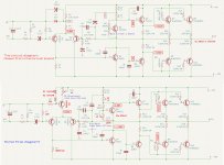
Hello everyone. Using a 1 Amp transformer with an AC 12/0/12 (DC 18/0/18) for testing, I obtained the results after making the suggested adjustments. please see the attachment

Hello everyone. Using a 1 Amp transformer with an AC 12/0/12 (DC 18/0/18) for testing, I obtained the results after making the suggested adjustments. please see the attachment
Last edited by a moderator:
Q5 doesn't appear to be conducting. Your test supply voltage is so low that there may be insufficient current flowing in Q1 to bias Q4 into conduction. The emitters of Q1 and Q2 look suspiciously the same.
In view of the low supply voltage, temporarily make 470 ohm. If the amp still doesn't show signs of life, report all the voltages you noted in the schematic above and:
output
base of Q1
base of Q2
base and collector of Q5 with respect to Q5 emitter.
Thanks.
BTW, I don't see any bypass caps on the supply rails. Adding them would be good practice.
Last edited:
Hello to all of you. There is activity on the amp. Without your suggestions and comments, it would not be possible to run the amp properly. Many thanks.
For of this modification, I was quite hassle to couple Q1 and Q2 Transistor. Rather, I make a bridge out of copper wire to allow the two transistors to share heat. It's a dumb idea, but I have gave it my best shot.
For of this modification, I was quite hassle to couple Q1 and Q2 Transistor. Rather, I make a bridge out of copper wire to allow the two transistors to share heat. It's a dumb idea, but I have gave it my best shot.
Attachments
- Home
- Amplifiers
- Solid State
- Please help me to solve the Unbalanced Bias voltage and The DC Offset