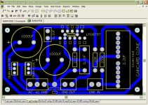
Wasin said:This is my inverted gaincard clone pcb
but I 'm not sure. Is it good for no HUM or any problem?
There are two things I do not like, as they may cause some hum:
1) AC is on the same pcb as the amp. IMHO the diodes should be on a separate board or place. Or at least more far away.
2) The main cap's ground legs have different trace paths, and I think they should be as similar as possible. Then take the mid point and wire to the star from there.
This is an opinion, as it has always worked for me, but I would put the star on a separate place. Bolted to the amp's metal enclosure (but isolated from it). The wall's ground should be tried before wiring it to the star, to see if it brings any harm to the hum.
Carlos
Re: Re: Please comment my Inverted Gainclone PCB
I agree with all your other comments, but I couldn't understand the meaning of this one. Can you please explain? Do you mean the lengths of the tracks from the two smoothing caps to the star ground point?carlmart said:2) The main cap's ground legs have different trace paths, and I think they should be as similar as possible. Then take the mid point and wire to the star from there.
You really want to have a link between the grounds of the two PSU caps as short as possible, then run a spur off this the the star ground. Quite high currents can flow between the caps, and this can induce noise into other more sensitive stages.
Got it now... it's very clear now. I was not doing this in my PCB design. I'll re-visit it and see how I can get this thing done. Maybe a jumper may be needed.pinkmouse said:You really want to have a link between the grounds of the two PSU caps as short as possible, then run a spur off this the the star ground. Quite high currents can flow between the caps, and this can induce noise into other more sensitive stages.
Thanks. 🙂
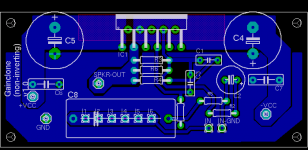
This is where I'd reached...
... but as you can see, I don't think I'm doing the right thing about the track connecting the two filter caps ground leads. Of course, this doesn't really affect the signal carrying tracks, because I have two separate grounds, one for power (labelled GND) and one for signal (labelled IN-GND). So the only noise that'll go from the charge/discharge currents of the caps to the signal tracks will be ones which are capacitively coupled from one track to another.
I am keeping a separate PCB for star ground, and intended to take two separate leads from the gainclone PCB to that one. And you'll also notice that there's no GND terminal for the speaker... I was intending to bring the speaker's return lead directly to the star ground PCB. Will this sort of thing work?
I'm wondering... will the ground link between my caps still be an issue considering I'm keeping the star ground off-board, and the signal paths don't mix with the power ground on my board?
BTW, if anyone wants my Eagle files for this, please just ask. 🙂
Attachments
The power caps on your PCB
Pinkmouse and others, am I making sense?
Looking at the filtering caps on your PCB, specifically from the ground-track point of view, I think you might find it better to rotate both your caps by 180 degrees. That way, their ground terminals would be adjacent to each other, and you could directly short them with a track maybe a quarter of an inch wide. (Yes, I think you need wider tracks at least for that one.) And then you can just draw one track from this fat one to the star ground.Wasin said:This is my inverted gaincard clone pcb
Pinkmouse and others, am I making sense?
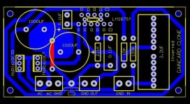
Re: How about this
Apparently, the charge/discharge currents on the ground track between the filter caps is so high and turbulent that it's best if it is not even allowed to touch the star ground. Therefore, maybe you can take the red jumper from the midpoint of your supply caps straight to the GND terminal where you connect the centre tap from your transformer. And take a separate track from this terminal to the star ground. That way, the charge/discharge currents between the caps will go straight to the transformer via a direct return path without actually going through the star ground. This is even more important in your PCB than in mine, because in my PCB, the signal ground does not go to the power ground.
I'm no expert, but I think this is closer to what was recommended. BTW, there's a ground track snaking up the left side of the PCB, which doesn't seem to have any connections. Why don't you remove it? And yes, now that I've understood your circuit a bit better, it appears that you're feeding the output of a transformer directly to your PCB. In that case, from what I've been told before, one more change to your ground tracks may be in order.Wasin said:How about this ground supply layout ?
Apparently, the charge/discharge currents on the ground track between the filter caps is so high and turbulent that it's best if it is not even allowed to touch the star ground. Therefore, maybe you can take the red jumper from the midpoint of your supply caps straight to the GND terminal where you connect the centre tap from your transformer. And take a separate track from this terminal to the star ground. That way, the charge/discharge currents between the caps will go straight to the transformer via a direct return path without actually going through the star ground. This is even more important in your PCB than in mine, because in my PCB, the signal ground does not go to the power ground.
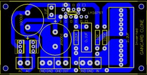
Khun Wasin,
Assuming the diodes are '2-in-1', then it seems to me that there's something very wrong with the rectifier section. I've always needed three of these diodes to make up a full bridge, and as it's shown, I suspect the -ve rail cap will explode.
My personal preference has always been to put the bypass caps from +/gnd, and -/gnd, not across +/-, esp. not just after rectification.
It's not wrong
It's not wrong on bridge rectifer
please Cheak Motolora MUR1610CT and MUR1610CTR datasheet first ....MUR1610 use for positve and MUR1610CTR use for negative.
and the cap that is cross V+ rail and V- rail is use for reduce noise
from power supply. It's not wrong too.
It's not wrong on bridge rectifer
please Cheak Motolora MUR1610CT and MUR1610CTR datasheet first ....MUR1610 use for positve and MUR1610CTR use for negative.
and the cap that is cross V+ rail and V- rail is use for reduce noise
from power supply. It's not wrong too.
The trace from the chip to OUT needs to be wider, high currents will flow to the speaker. And also the OUT-ground needs to be wider, because the same currents will go here also. And another thing; the OUT-GND must go to power-ground not signal-ground.

- Status
- Not open for further replies.
- Home
- Amplifiers
- Chip Amps
- Please comment my Inverted Gainclone PCB