Hi all.
I've been working on this design for a while and I would like any comment's you've got.
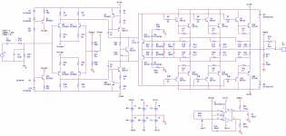
I guess that the schematic is know material to most of you and the only odd thning is the VI-limiter around Q1, Q12, Q14 and Q25 and the components around them.
The supply for the output (Vcc36/Vss36) is a 620W torroid. The 42V and 12V supply´s are regulated.
I'll build 4 of these (lot of components, -I know..) and bridge them to make at stereo amp of approx. 2*175W
The prototype (without the VI-limiter) is working fine and is very stable. I removed the input filter and feed the amp with a squarewave and there where no signs of overshoot or peaks onthe output.
I've got a complete PSpice model of the amp if any of you want it?
Most of the design is taken from: "Introduction to electroacoustic & Audio amplifier design" by Leach, and from schematics found on the www
The things I´m wondering about:
-What difference would base-resistors in the diff.-amp do?
-How do I calculate the resistor values around the output-stage?
More to come. I hope to make PCB's in a week or so.
TroelsM
I've been working on this design for a while and I would like any comment's you've got.
I guess that the schematic is know material to most of you and the only odd thning is the VI-limiter around Q1, Q12, Q14 and Q25 and the components around them.
The supply for the output (Vcc36/Vss36) is a 620W torroid. The 42V and 12V supply´s are regulated.
I'll build 4 of these (lot of components, -I know..) and bridge them to make at stereo amp of approx. 2*175W
The prototype (without the VI-limiter) is working fine and is very stable. I removed the input filter and feed the amp with a squarewave and there where no signs of overshoot or peaks onthe output.
I've got a complete PSpice model of the amp if any of you want it?
Most of the design is taken from: "Introduction to electroacoustic & Audio amplifier design" by Leach, and from schematics found on the www
The things I´m wondering about:
-What difference would base-resistors in the diff.-amp do?
-How do I calculate the resistor values around the output-stage?
More to come. I hope to make PCB's in a week or so.
TroelsM
Attachments
good work there
🙂 🙂 🙂
hi TroelsM,
theres no problem with your work
the output stage is just a bit messy. why not making it the driver stage and with the output devices paralleled.
😀
but this thing will work, if you want your output stage to be that way
then no problem 😀
one more thing
you need not have two supply rails, for the VAS and the output stage respectively🙂
these type of supply rails are recommended for FET output stages mostly.
nice job,
hienrich
thanks
Hi.
The many driver transistors are there to distribute the load of the TIP's. I dont know if it's necessary. Maybe I'll remove some of them and use 1 driver for all 3 TIP's.
I can't afford to much space for cooling of the drivers and I guess that 3 drivers will be able to get rid of the heat better than 1 would?
How will the current-sharing between the TIP's be affected by 3 or 1 driver? I guess that 1 driver is the best solution, but what do you think?
I was hoping that I did'nt have to measure the Hfe og all the transistors, but will it work?
The higher supply for the pre-stage is not necessary, but i'ts my understanding that i'ts the best solution for a number of reasons.
TroelsM
Your design look fairly reasonable but there are a couple of unusual points I noticed:
Your output base resistors (R11 etc) are quite low and your drivers are working fairly hard to get the outputs into conduction. Using low values here help output device turn-off but if you are using TIP devices (they not fast) then I dont know why you need 33 ohms there. You have slow output devices and then you use a technique to make them as fast as possible, but you take the disadvantages of the technique. If you are worried about output stage bandwidth then dont use the TIP devices. I dont think output stage bandwidth should be a real consideration considering the inductor at the output. It is a lowpass filter anyway. Personally, I'd use a 100 ohms there (placed around the emitter resistors) and have 1 driver (maybe a different type) for all 3 output devices. Less pieces to worry about...
I think R4 and R50 dont serve any purpose at all. I know it looks 'better' but it makes no difference. If i remember correctly the Douglas Self site mentions this somewhere.
Personally I dont understand the fascination many people have with these 'double LTPl' input stages. I think a normal LTP with a current mirror is really the best. But I admit the double LTP stages look nice on schematic.
Using multiple supplies for 1 channel amp always seems to me to be bad design. Better to redesign the amp to use 1 supply. Its a very expensive way to get an amp that is just a little bit easier to design.
These are just some things I noticed. The design looks good and will probably work just fine.
Doug Eleveld
Oh yeah and your comment about driver emitter resistors: You dont need to match output devices if you use only1 driver. If you place the emitter resistors around the output emitter resistors. The voltage drop over the output emitter resistors helps balance output device current for different output device gains.
Doug Eleveld
Doug Eleveld
I think it is very good... i like that simetrical designs.
But tell me, that's the question appeared into my mind.
How it sounds.... in comparison with other known sound you have or used to compare.
When i see those double simetrical...i always imagine some 6 dB reduction of bass.
That's the reason of the question.
related the circuit...the darlingtons you constructed was great...also the heat distribution in many output transistors were clever.
But tell me...the sound...please.
nanabrother@yahoo.com
Carlos
Hi,
the current protection on the VAS also limits dissipation on the output protection. You can change Q12&14 to fast, low power types. Q12 & 14 also require stopper diodes in series from the drive lines (collectors of q11 &15)
I don't know what D5&6 are doing?
I have seen C4 & C5 replaced with a single cap NOT connected to the output. You should leave lots of room and extra holes in the pcb for different sizes of C4&5 to change the time constant of the VI protection. You may want to go as high as 100uF to allow peaks to pass through without limiting.
I agree the idea to ditch the integrated darlingtons.
regards Andrew T.
hi TroelsM
i like it very much
including r4&r50- they equalize R*Cmiller
including separete rails-they always improve sound and you can get rid of "dual mono" and run normal stereo
including separete drivers-they work at 3 times lower currents compared to one driver, it is good with more output bjts to be driven by lower power (read:faster and higher beta) drivers
the only thing I am wondering about is frequency compensation..
enough??
regards
one more thing:
do you use regulated supply fo VAS?
I think it is worth doing and easy even with LM317/337
do you use regulated supply fo VAS?
I think it is worth doing and easy even with LM317/337
Hi TroelsM,
IMHO the time constant of the DC-servo is too low. Its just
100ms which is 1.6 Hz. Better use 470n caps.
The TL071 is not the best choice for servocircuits, its a poor,
outdated device. I would use a fetopamp with lower offset
voltage.
Its a pleasing design though.
Uli

IMHO the time constant of the DC-servo is too low. Its just
100ms which is 1.6 Hz. Better use 470n caps.
The TL071 is not the best choice for servocircuits, its a poor,
outdated device. I would use a fetopamp with lower offset
voltage.
Its a pleasing design though.
Uli
6db loss
How it sounds.... in comparison with other known sound you have or used to compare.
When i see those double simetrical...i always imagine some 6 dB reduction of bass.
😀 sir DX,
hi
weve got the same points when it comes to this kind of
circuit "mirror image" or double symmetrical.
the same circuit topology as the "LEACH" , in which I've also tried
making it . There is the lack of dynamic bass.
As what some diyers also said in some threads
do you have Any known circuit which you have tried and tested, that you can also share to us.?
Pls. don't forget to attach your favorite or your prefered circuit.
I'll be happy to keep or try them also.
😉
if that circuit is large for the thread. you might just email me.
I'll be happy waiting...
😀 😀
TroelsM:
for your driver transsistors try MJE15030/MJE15031,
MJL21194/MJL21193 for the outputs, these are real
kicking ones....
regards,
macweb
e-mail: sp_bagnol@yahoo.com
Doug Eleveld:
i don't get it. Is my solution ok, or should I place the resistors different? i would like to use 1 driver for all 3 TIP's, but right now I'll stick to the seperate drivers.
AndrewT :
The diodes in the curcuit are there to protect the transistors from voltage spikes and reverse voltage.
hienrich:
It's not really an option to change the transistor-types as I'm using the ones that are available to me. Because of the large number of transistors it will be pretty expensive to change to another type.
uli:
Yes I'ts a terrible opamp, but it seems to do the job and I'ts cheap. You're right about the timeconstant.
darkfenriz:
"the only thing I am wondering about is frequency compensation..
enough??" come again. I don't get it.
What about the base-resistors in the input-section? Should I use them or not? As far as i remember it has something to do with making the internal Rbe more linear?
TroelsM
Hi TroelsM,
I think you design will work just fine. My comments are just about they way I would approach your design.
I think 1 driver for all the output devices is a more elegant solution. If you connect R11 to the other side of R24 (the output node) is the way most people do it. It might also help linearity by reducing current variation in the drivers but I'm not sure. Then you can parallel output devices, but each of them have to have thier own emitter resistor. Most people use 100 for R11 too.
You are right that using 1 driver means the drivers will have dissipate more. If you are worried about overloading the drivers you have available then your solution of 3 drivers should work. Increasing R11 would lower dissipation too though.
As far as compensation goes I can give you no meaningful advice. I prefer to overcompensate, sometimes grossly, when designing and lower the compensation cap when you know the rest works. That being said I think 2p seems too small, but I could be wrong. Simulation should give a reasonable start value.
I cant imagine how base-emitter resistors in the input section would do anything useful. If it helped linearity it would only be a very little bit. You could achieve that better by increasing the LTP emitter resistors and increasing tail current to get the same gain. But why are you worried about linearity of the input stage? IIRC most nonlinearity is in the output stage anyway.
Why dont you use a current mirror as a load for the LTP? Instead of R3 and completely useless R4.
I'll also be showing a design here and asking advice in a little while too. I'd appreciate it if you would comment on it.
Doug Eleveld
initially I would give somthing like 47pF millers or even more and decrease this value while observing square wave response...
maybe these 2pF are enough to eliminate oscilations but you may expect some ringing of the square wave
maybe these 2pF are enough to eliminate oscilations but you may expect some ringing of the square wave
Hi TroelsM
I still cannot understand the need for D5&6.
Q12&14 monitor the voltage drop across the emitter resistors.
Q12&14 emitters float on the output voltage. I cannot see D5&6 doing anything, can you explain.
I think you need diodes on the collectors of Q12&14.
regards Andrew T.
I still cannot understand the need for D5&6.
Q12&14 monitor the voltage drop across the emitter resistors.
Q12&14 emitters float on the output voltage. I cannot see D5&6 doing anything, can you explain.
I think you need diodes on the collectors of Q12&14.
regards Andrew T.
Hi,
I'm not sure of my method but I have just checked the short circuit current limit.
negative current will limit at 6.4a to 7.3amp and positive current at about 7.4a to 8.7a peak values.
At these currents the heatsink will have to dissipate about 600watts.
How does your amp switch off to prevent rapid and severe overheating?
regards Andrew T.
The cut-off-current is dependent on the output voltage
As the output voltage is setting the current-limit you cannot talk about an "absolute" currentlimit. It will (hopefully) limie as follows:
Vout = 0V -> Ilim = 3A
Vout = 30V -> Ilim = 20A
TroelsM
As the output voltage is setting the current-limit you cannot talk about an "absolute" currentlimit. It will (hopefully) limie as follows:
Vout = 0V -> Ilim = 3A
Vout = 30V -> Ilim = 20A
TroelsM
Hi,
short circuit current limit is far above 3amps. When in short circuit mode the voltage swing on the output is very close to zero probably less than 1volt.
You need 0.6v to 0.7v to turn on the protection transistors.
I have used the following method:-
Consider +ve limit current for a moment & using the step up ratio of (120+330)/330 times 0.7v, you need 0.955v at the emitter resistor. Divide by 0.33r gives an emitter current of 2.89a. With 3 // outputs the short circuit current could be as high as 8.68a.
If the max current is also out by this sort of range then your set points for your protection are far above expectations.
regards Andrew T.
- Status
- Not open for further replies.
- Home
- Amplifiers
- Solid State
- Please comment "my" design