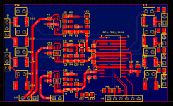
Hi,
i would like to ask for your support, to improve and check my design of PGA4311 volume controller board. This just my third in creating PCB designs.
The main goal ist to replace a existing PT2258 board, because of its sound and electrical parameters, that doesn't fit well to the needs. The DC-Offset on VDD/2 at the outputs, caused by the unsymmetrical power supply, is the primarily reason.
I had chosen the 4311 because of the 4 channels i need, low dc offset at the outputs and generally better parameters. Source are two of the cheap PCM1502 dac boards with 1kOhm Zout, sink is a preamp board for each channel, with 50kOhm Zin. The preamps have the possibility to adjust DC-offset. It would be fine to do without any coupling capacitor in signal-lines.
The board is for Layer, buttom layer is ground plane DGND, 3rd layer has a copper area for AGND, 2nd layer is mainly used for analog signal, top layer all other stuff. The footprints for coupling capacitors are for some experiments and optional to use. Also C19 is optional, i don't understand its function well. Other questions are: Are resitors in the analog signal lines before and after 4311 necessary, if coupling C are in use? What can i do to improve EMI/EMV?
The type of connectors are not fixed an will be changed to more suitable type. SPI out for daisy chain will be added.
Pleas roast me with some critics and hints. Thanks a lot.
Attachments
Digital ground and analog ground are normally confined to different parts of the board so they don't couple to each other. Having them in a sandwich will add to capacitive coupling of digital ground noise into the analog section I fear.
Why not use a classic signal-ground-power-signal layer stackup?
Figure 6 in the datasheet suggests a layout - go with this...
Why not use a classic signal-ground-power-signal layer stackup?
Figure 6 in the datasheet suggests a layout - go with this...
5cm underneath the PGA board is a an other board, that contains a uC, and handles also digital signals like i2s, spdif, spi ..., it is a proto build on a veroboard.
The ideas was to use the bottom layer as DGND and shield, i fear to build antenna with traces on bottom. From my point a view (i am a beginner), there are just a view traces that are real "digital", but i can also follow your point.
What do you think about the idea, to switch with DGND also on the 3rd layer, and use bottom layer just as shield "SGND", maybe with some jumper to experiment with connection to different GNDs.
Meanhile have deleted pull-downs R8 and R9 --> will move to uC-board, and added output connectors for power and SPI, where im not sure to plan in some series resistors for termination.
I'd go with the datasheet in case it matters. You normally want a power plane or layer if you've gone for 4 layers its really convenient to use one. A nearby board is only very weakly coupled compared to plane-to-plane coupling. The layer 2 ground planes will shield the top layer, you shouldn't need two shields.
I'd worry more about noise currents in the ground planes - typically a digital and analog ground plane are shared at one point only, usually underneath a DAC or ADC, so there is no ground loop between them. The datasheet shows a decoupling capacitor between analog and digital which is also doing this, so you want to connect the ground planes under this capacitor really.
Digital noise currents flow around in the digital ground plane and digital supply traces/planes, if you place a plane parallel to this it will have equal/opposite currents induced in it (think how wireless chargers work)... There are three methods unwanted noise spreads around, capacitive near field, magnetic near field, and electro-magnetic waves, its hard to optimize for all three, but the chip manufacturer will have tried to get the best performance out of their chip and put that design in the datasheet suggested layout for you...
After your post, i had read some articles about layer stacking and coupling effects on PCBs. Thanks for these hints.
So i have changed the layer stackup mainly to the proposed one, with some exceptions for analog signal lines. From my point a view, the solution to keep it away from the other things, i have some pain to route them on the bottom layer.
For the digital signal lines some optional series resistors are added, they can be 0Ohm - 100Ohm to prevent overshoots in the signal.
The plans was work with seperateted grounds without any connection on this board, this should be done on the power supply part, nevertheless a footprint for a coupling C or R is added also for optional use.
Have a look plaese.
