I have Pete's Compactron Triple triode push-pull driver PCBs Push-pull driver board as well as his AB2 buffer boards A2 Buffer to build a 6L6GC AB2 amp.
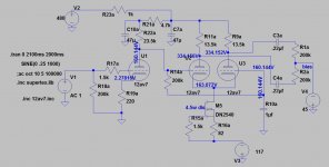
I've completed a draft of the amp using LTSpice. I am posting the driver board schematic here for comments. I am using a 6AK10 triple triode, which seems linear and a good choice. It has similar characteristics but more linear, than a 12AV7. I did not find a model for 6AK10 in LTSpice. I attached the 6AK10 data sheet.
I've attached the LTSpice file as well as two .inc files required to run this simulation. Replace .txt with .inc to run.
Please comment.
As this thread progresses, I will add the A2 buffer board, the power supplies, and output stage. Thanks!
Attachments
Last edited:
Tom, I missed this when you posed it, but I've got plans to build about the same thing this winter. I got Pete's compactron driver, and a2 buffer boards last year, too.
Same driver, but I think I'll use some kt88-like tubes in triode or UL for the output, ab2.
From what I can see, you've got your schematic drawn incorrectly, though. Your LTP isn't configured the way I've seen before. You have signal going to both grids, and usually the 2nd grid is grounded. It's DC coupled, while pete's is AC (through a cap). But I have to admit, I don't know if yours is wrong, or if you know how to configure an LTP more ways than I do. If you think yours could be wrong, I'd say look up the difference between AC and DC coupled LTP's.
I configured it thusly: The Valve Wizard
It seems to work in simulation (famous last words I know). I wanted to go DC coupled even though I know the board is for AC coupling.
It seems to work in simulation (famous last words I know). I wanted to go DC coupled even though I know the board is for AC coupling.
From what I can see, you've got your schematic drawn incorrectly, though. Your LTP isn't configured the way I've seen before. You have signal going to both grids, and usually the 2nd grid is grounded. It's DC coupled, while pete's is AC (through a cap). But I have to admit, I don't know if yours is wrong, or if you know how to configure an LTP more ways than I do. If you think yours could be wrong, I'd say look up the difference between AC and DC coupled LTP's.
Unless he revised it, there's nothing wrong with the schemo as presented. His design is identical to the topology I used for the front end of the Vixen design: a SE pre DC coupled to an LTP (different types used here: 6J5 + 6SL7). There were no problems with it.
The 2nd grid is AC grounded, but DC isolated. The resistor spanning the LTP grids applies the same VDC to both grids, and the capacitor to ground is the AC ground.
Nah... its OK
I think that part is OK (the bold part). Note the 1 μF capacitor acting as a DC-lifting A/C signal ground on the right triode? Trickle-charged by the 200°K resistor, it will basically be a DC point, self leveling with the average input on the other half of the LTP.
My bigger question has to do with the OUTPUT of the LTP - it is differential output, yet it seems to be summed with a couple of resistors. Don't understand what the point is there. To me it seems that this will effectively null all the "goodness" of the LTP. It is a phase splitter par excellence, and to sum the differential outputs removes the signal, and leaves nothing but the distortion!
Anyway, I'm just a dumb old designer. What do I know.
GoatGuy
From what I can see, you've got your schematic drawn incorrectly, though. Your LTP isn't configured the way I've seen before. You have signal going to both grids, and usually the 2nd grid is grounded. It's DC coupled, while pete's is AC (through a cap). But I have to admit, I don't know if yours is wrong, or if you know how to configure an LTP more ways than I do. If you think yours could be wrong, I'd say look up the difference between AC and DC coupled LTP's.
I think that part is OK (the bold part). Note the 1 μF capacitor acting as a DC-lifting A/C signal ground on the right triode? Trickle-charged by the 200°K resistor, it will basically be a DC point, self leveling with the average input on the other half of the LTP.
My bigger question has to do with the OUTPUT of the LTP - it is differential output, yet it seems to be summed with a couple of resistors. Don't understand what the point is there. To me it seems that this will effectively null all the "goodness" of the LTP. It is a phase splitter par excellence, and to sum the differential outputs removes the signal, and leaves nothing but the distortion!
Anyway, I'm just a dumb old designer. What do I know.
GoatGuy
From what I can see, you've got your schematic drawn incorrectly
Looks fine to me. 1uF seems large, I might be wrong but I think a .1uF would be sufficient ?
The schematic will work as drawn. The LTP design is a common guitar amp variation. The Valve Wizard site is written from a guitar amp standpoint, but this LTP will work for a HiFi design as well. It does require a good quality cap that works across the entire audio range, but makes life easier with DC coupling.
The resistors on the output are the grid bias resistors on the output tubes.....or the gate resistors on the mosfet boards. They are needed for the simulation to be accurate.
Since this design IS using mosfet drivers, I would increase the value of those resistors and decrease the coupling cap values to keep the time constant about the same.
Those resistors are part of the load on the LTP, and you will get more gain and lower distortion with a lighter load. Mosfets don't have "maximum grid circuit resistance" specs, so the 200K's can be 470K or 1 Meg.
You need to lower the coupling cap a bit to keep the time constant reasonable. Otherwise setting the bias can be a time consuming and tube melting affair. I once built a mosfet coupled amp with 1 uF caps (I have a box full of 1 uF Multi Caps) and 1 meg resistors. Turn the bias pot and it takes SECONDS for the change to take effect. By the time you realized that you turned it too far, your output tubes are glowing red.
Doh, sorry... For some reason the 200k r14 threw me off (used to seeing 1meg+ there on old dc coupled amps), and I was the one getting mixed up between ac and dc coupled... (got some conversation going, at least)
Thanks for the comments, everyone!
I will digest them and revise the driver circuit in the next day or two and post it here. I have already draft-designed and simulated the whole amp but am starting here with the driver circuit.
Once this is discussed enough, I will show the AB2 drivers, the components I selected, and how I plan on getting the + - power from the power transformer I have.
- Status
- Not open for further replies.
- Home
- Amplifiers
- Tubes / Valves
- Pete Millett Compactron Triple triode push-pull driver PCB for 6L6GC AB2 amp