HI,
the circuit in #18 won´t work.
There are several issues.
1- The way You drew the signal current sources I1 and I2 their currents enter the sub-circuits in phase.
The subcircuits beeing complemetary You will now sense a output voltage.
If the signal current sources are drawn the correct way, there will be no output voltage at all.
2- If I1 and I2 were the outputs of PCM1795 or PCM1796 DAC the offset curent of -3.5mA would be missing.
Adding that current would lead to greatly differing bias currents through the subcircuits.
To balance the currents through the CFPs all four constant current sources -formed by J1 to J4- needed to be tuned individually to different current values.
3- The collector resistors of the CFP masters are a bit large (3k and 3k5)
It´d be better if the Masters run on more current, say ~500µA-1mA (~1k)
Also the compensation networks -if necessary anyway- seem a bit too capacitive.
I´d guess around 100p would be more than enough.
You could maybe get it to work in that You use two of either the upper subcircuit or the lower subcircuit and connect the two output cascodes by a common CCS towards the other supply line ... see attchement.
Of course does this circuit also offer two out-of-phase Outputs which may be used SE or balanced.
Note:
This hasn´t been tested in praxis, just qicksimmed.
As two high-impedance cascodes work onto a high-impedance CCS, small imbalances of the cascode currents to each other and the cascode-to-CCS currents lead to output offset.
I´d rather choose separate CCS for both branches which could then be DC-servoed.
Also for pure convinience, cost and easy sourcing I´d rather choose bipolar CCSs for an all bipolar circuit.
jauu
Calvin
Attachments
Last edited:
Hi Calvin,
you are right.
the current sources may drawn wrong but you can let work one with 0° phase and the other is programmend with 180° as can be seen on the shematic.
Yes I1 and I2 are the symmetric output of the PCM1796.
I forgot to mention that i would use a separate ccs to cancle the offset and if you do so no problem with current balancing.
The collector resistor seems indeed high. I started with 1k and if you increase the value you get little bit lower THD.
Same with the compensation network, i started with lower values like 50p and it seems more stable with 350p and 50ohms.Nice decreasing curve with no peaks.
But i have to say it´s just simmulation and one of my first more complex cirrcuits and i´m fare away from being a profi(i´m just landscaps gardener).
I will have a look at your suggestions and the cirrcuit and try to learn more about the topic.
Thanks a lot Calvin for your comments.
May we see us at the Frickelfest 2015(hope so)
Roland
Hi,
The polarity of the current sources is defined by the arrow marking, similar to the + and - markings of the voltage sources.
In #18 and #20 the arrow of I1 points towards gnd, while that of I2 point away from gnd.
For same current values they are out-of-phase.
Adding the 180° phase shift puts them in in-phase condition.
As the PNP part of the circuit works out-of-phase to the NPN part -which is what the term pushpull stands for- You get a output voltage dropping over the 500R resistor, due to the difference in output currents of upper and lower part beeing routed through the resistor.
If the input currents were out-of-phase instead, the output currents of upper and lower part would be in-phase and no difference current occurs that could be routed through the resistor, hence no output voltage.
If You need out-of-phase output currents with out-of-phase input currents, two identical circuit halves are required.
Pushpull circuits are fine for signals referenced around 0V (or 0A).
The elegance and beauty of the SE stage shines with asymmetric signals.
In its simplest form it requires only one current source to cope with the DACs offset current and to bias the circuit correctly at the same.
Changing to a pushpull circuit puts away with this multifunctionality.
Additional parts for another CCS are required.
If that resulted in an advantage it might be ok, but here nothing is gained from the extra circuit complexity.
Instead it is quite probable that the circuit becomes less stable, or gets noisier.
Certainly more complexity just increases the failure- and breakdown probability.
jauu
Calvin
Last edited:
I'm wondering, is there any pro for using balanced signal, then unbalancing it to single ended, over just using one output? If is what circuit should i use? Differential amp, then a emitter(or source) follower? Use feedback, or not? Final question: what about filtering? Just passive RC, or LC filter between I/U and buffer?
Thats a lot of questions...
Thats a lot of questions...
Hi,
in theory the even distortion parts of the DAC chip itself would cancel, giving overall lower THD figures.
This requires that both outputs of a single stereo channel are loaded the same.
As for most cases each single current output of the DACs is already so low in THD that in praxis it doesn´t matter.
The I-V conversion and buffering will usually bethe dominant THD contributor anyway.
What imho does matter is the way the I is converted to V and how many devices are involved in that process.
Even the simple common Base structure (with a single CCS and the Riv connected towards a supply line) can achieve -80 to -90dB THD at 0dBfs.
Most commercial specs are sweetened as are at taken at -6dBfs -- take care of that!
Such low THD figures would already be very ok for high-gain, high-feedback OPAmp circuits at 1kHz.
Above 1kHz their THD over frequency plot typically rises sharply due to decreasing feedback factor and other effects.
For the simple common Base circuits, running without feedback, resp. under openloop conditions, the figures are very good and certainly low enough to be considered negligible.
The increase of THD typically occurs towards higher frequencies and is less prominent.
Also a often neglected point is, that OPAmp circuits input impedance rises considerably at already low frequencies.
Input impedance should remain as low and constant as possible up to a couple of MHz (at least to the frequency the DAC chip clocks its outputs).
The feedbackless common Base circuits -while on a generally higher impedance niveau- behave more constant in this regard.
The CFPed common Base then allows for input impedances in the milliOhm range up into the MHz range.
The folded cascode becomes interesting imho only if You want to avoid a AC-coupling cap.
Keep in mind though that You might need -besides the anyway greater parts number count- a DC servo, that in itself requires at least two caps.
If you for example take the circuit from #7, and You use Buffer stages with very high inpt impedance (say JFET-Inputs) C1 and C21 may be the only AC-coupling caps.
As they see a high and defined load impedance they may be chosen quite small in value, down to ~220nF.
A value range where You can choose from first class film types.
The typical value for DC-servo caps is no smaller (~1µF).
DV coupling the Buffer and using a output cap at the Buffer output instead, required much larger cap values, as the load impedance is not defined and could be quite low.
In short, I´d opt for the simpler circuit, as the more complex circuits don´t offer clear advantages, but are more complex, costier, less easy in handling and stability andsoon andsoon.
jauu
Calvin
Last edited:
Correct me, if I'm wrong: if I use a high impedance device on buffer: jfet, or depletion mode mosfet, I can do filtering with only a cap to the ground before buffer? What is CFP? When did you come with folded cascade? For what and where? I guess my english is limiting me now...
Hi,
If you for example take the circuit from #7, and You use Buffer stages with very high input impedance (say JFET-Inputs) C1 and C21 may be the only AC-coupling caps.
In #7 there are no Buffers shown.
They´d be connected to the IV-stage at (or "behind") C1 and C21.
The folded cascode was introduced with DCD3500rg´s post.
It is used as a so called ´Level-translator´.
If You look at #7, You´ll see that there is a voltage potential at point ´dc´.
Between point ´out´, that is at 0V dc level, and point ´dc´, the cap C blocks the dc, or AC-couples to the output.
Now if You look at #21, You´ll notice that where You´d expect Riv, there´s now the CCS J6/R18.
The AC-current signal that entered the circuit by ´inp´ and wandered upwards through Q11/Q13 is now directed ´to-the-right´ and through the transistor array Q14/Q15 (added on top of a dc bias current).
You see the emitter potential of Q14 at +5.7V
The current through Q14/Q15 flowing into the node ´out2´ divides into a current through R20 and a current through R10 and the CCS Q21/22.
In a fully SE circuit topology there would be no connection from the CCS to the ´right hand side´ through R36.
Now by varying the dc-current value through R10 You can decide how much dc-current is left over through R20.
If the dc-current through R10 is made identical to the dc-current trough Q14/Q15, there´d be no dc-current through R20, hence no voltage drop, hence ´out2´ would be at 0V potential.
Under AC signal conditions, now all AC-current must route through R20, creating a AC-voltage drop, the signal voltage.
So R20 has become our Riv with the advantage that the output signal is centered around 0V, instead of the ´dc-potential´ as in #7.
In other words:
The two CCSs (J6 and Q21/22) and the transistor array Q14/15 in #21 provide for the same function as the single AC-coupling cap in #7.
The folded cascode has one major advantage though.
The Riv is connected to signal gnd instead of a supply rail, and as the CCSs shield the common-Base transistors as well as the cascode-transistors against noise and ripple on the supply rails, the power supply rejection ratio (PSRR) is alot higher.
This reduces the requirement for a first-class quality supply.
Providing for a quiet and constant supply rail is no hyperspace technology at all.
I´d opt for the simpler circuit of #7, as I regard a decent clean and noise-free power supply a must anyway.
Less parts, less hassle, and Imho better sound also.
But feel perfectly free to choose Your poison.
jauu
Calvin
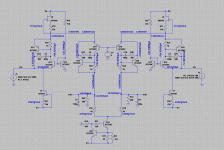
CFP stands for complementary feedback pair also known as sziklai pair.
And thats what it look like.

And that is a folded cascode. Two transistors in series a p-channel and a n-channel.

Thats what i did in my cirrcuit with two CFP in series.
And thats what it look like.
And that is a folded cascode. Two transistors in series a p-channel and a n-channel.
Thats what i did in my cirrcuit with two CFP in series.
Hi,
now i decicded to built Calvins "simple circuit" shown in post 7.
I will use as power supply the ccs/shunt regulator wich supplys the "Paradise" phonostage because i have them on hand like the Calvin buffers.
It delivers +- 18V, i only have to do some small canges to the I/U stage.
I thought if the regulator is good for a phonostage it will be allwright for the I/U converter plus the Calvin buffer.
But i have still some questions: to my understanding i normally dont need any capacitor in the supply rail because of the regulationbehavior of the ccs/shunt regulator.
Is it still usefull to put some caps on the power rail or a CLC filter (like in the circuit from post 7) to decouple U/I stage from the Buffer?
I will use mainly through hole components but for the coupling cap may be SMDs because they can be really small.
What do you think about Wima pps caps? Or there are better caps ?
Any suggestions on it?
Which through hole resistor for the Riv is the best solution?
Greetings
Roland
- Status
- Not open for further replies.
- Home
- Source & Line
- Digital Source
- PCM1796 I/U stage for CD/DAC