Hi
I know, that this topic is discussed everywhere, but it all makes me only more confused. I know basic electronics, but I/U conversion is a rocket science for me now(except simple passive and opamp active). I have Yamaha CD-S1000 which has PCM1796 DACs, built quality is excelent, but sound is thin and forward middle. I was looking at service manual and I blame analog stage, that has like a milion filters on it, which probably screw up phase responce.
So I want to do some research, ask you guys for advice and hopefully built a proper, hi quality analog stage to my CD.
First thing: discrette, or opamp based? With knowlege i posess I'm tilting towards opamp one, then unbalancing stage, with simple one stage RC(LC maybe, why?) filter. I would like to have option of having either balanced, and unbalanced option. This CD has dual mono DAC stage, but i think i will just use a half of each PCM, I'm not convinced, that using 4 outputs is worth a buck...
I'm not convinced, that those discrette buffers are really needed? What is their purpose? LT1007 is claimed to have 21mA pp, so it is enought i think.
Hi,
OPAmps are fine for convinient use.
And as they are cheap and easy to implement and IC suppliers assist with Application notes You find them in most commercial devices in vast numbers.
Besides the I/V conversion they are also used for analog post-filtering, balanced-to-SE conversion and output buffering.
If the DACs are oversampled to 192kHz (which is a quasi standard) the analog post filtering may be omitted with.
Also the balanced-to-SE conversion may be omitted with.
Both measures do away with parts and circuits which only serves Datasheet figures, but spoil sonics more often than not.
If You want natural authentic sound discrete is the way to go imho.
Search for 'Jocko' and 'current conveyor' for circuits.
The Jocko is a very simple, low parts count I/V converter circuit with reasonable low distortion and excellent sound.
It is perfectly suited to current sourcing DACs like the PCM179x series.
Basically one single transistor wired in common base topology serves as 'current buffer'.
This means that it provides for the low impedance (virtual ground) the DAC wants to see and at the same it supplies the very high impedance of a current source at its collector output.
This collector output feeds a single resistor that does the I-to-V conversion.
In theory the conversion resistor may be as high as You wish for, generating voltage levels way above line level, and that could even be used as high power DAC.
The voltage generated by the resistor is AC coupled to the output.
In praxis a classic voltage buffer should be used to drive the output.
Here a single transistor may suffice also, for example a JFET.
Noninverted and inverted DAC outputs can be treated the same.
For balanced output use both I/V converter outputs, for SE just use one of them.
Your signal path can't be much shorter and straighter than that.
As transistors typical easy to source and cheap 'audio' candidates like the BCs are suitable, nothing fancy or exotic.
Same or similar transistors may be used for a voltage Buffer ( for example for a diamond structure), keeping sourcing parts easy.
Sound is of course a issue of personal taste, but those simple discrete circuits offer so much more livelyness, authenticity and realism, some would say 'analog sound' that I doubt anybody who could listen to those would ever switch back to OPAmps.
jauu
Calvin
To answer the question above: the buffers keep the opamp very lightly loaded and more deeply biased in class A (the inherent offset to the pcm179* already helps there).
To my ears, it certainly sounds as good or better than the simple discrete stages. I've yet to try a transformer based I/V though.
To my ears, it certainly sounds as good or better than the simple discrete stages. I've yet to try a transformer based I/V though.
@00940
Thanks for information 🙂
@Calvin
This is very interesting project, sadly i don't understand perfectly how does it work. Also Jocko said, some tuning might be needed, as for triming R4 i would go with potentiometer, but regulation of CCS is much more tricky.
Q3 and Q4 are the CCS, how to calculate their current?
Q2 is base grounded amplifier, through Q1, to make Q2 emiter at ground level? Ue of Q2 is the same like Ue of Q1? How could one calculate and correct the bias of this stage.
I lack a lot of knowlege sadly 🙁
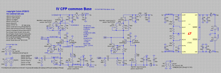
Hi,
attached is a reduced schematic of a slightly different to the Jocko IV-converter.
The differences are:
- PNP common Base instead of NPNs --> Allows for lower dc-currents of the current sources, hence less heat power. SMD devices useable.
- The IV-conversion Resistor Riv is connected directly to the transistor´s collector --> eliminates one current source, gives stable working points
- CFP-structure of a PNP/NPN --> gives much lower input impedance and lower THD, Input offset nulling becomes easier as both NPNs may run on same and very low bias currents.
- CCS made from a NJFET --> lowest parts count, easy to tune, lowest noise.
For the understanding of the circuit You need to know Kirchhoff´s Law.
It simply states that the sum of all currents flowing into and out of a node is 0.
Or in other words: What goes into a node must come out of the node.
For the Node ´in´ this are 3 currents.
1st the current coming from Vpos through the CCS made up from the JFET flowing into the node.
2nd the current from the DAC output connected to and flowing into ´in´ and
3rd the current flowing through the PNP/NPN and Riv towards Vneg.
or: Idac+Iccs = Iriv
The Iriv leads to a voltage drop over Riv of: Riv x Iriv.
If Idac=3.5mA and Iccs=0.5mA then Iriv =4.0mA.
If Riv=1k5 then Vriv=6.0V.
If Vneg=-15V then Vdc=-15V+6.0V=-9,0V.
If now Idac swings around -3.5mA by +-2mA, then Iriv swings around 4mA by +-2mA and Vriv swings around 6.0V by +-3.0V, resp. Vdc swings around -9.0V+-3.0V
Cap C ac-couples the signal to the output, hence Vout=+-3.0V, which equals ~2Vrms.
The second Attachment is a completely dimensioned circuit for one stereo channel of a PCM1795 or PCM1796 in stereo mode.
Noninverting and inverting signal outputs may be taken single ended or balanced.
Balanced just gives double the output voltage and output impedance and cancels out the even harmonics.
In single ended mode the second channel output simply remains unused/open.
Each of the PCMs DACs supplies for -3.5mA offset current and up to +-2mA signal current
If outputs are combined as in mono mode the Idac current values simply double and Riv may then be halfened for the same output voltage (~2Vrms).
What is only missing here are output Buffers to drive cables and attached devices.
jauu
Calvin
Attachments

Last edited:
Wow, thank you for this!
I can't find those SST4391 fets, can i use BF245, or 2SK170 instead? I have them on hand. Also values of trimpots, they should be like resitors in series with them?
R0 and C0 between Q2 emiter and base are the transistor internals, right?
As the buffer: I guess, that B1 will be enough? 😉
I now understand how does it work: I look on youtube for tutorials, also your postwas very helpful, especially Kirhoffs law reference.
If it sounds thin, You must add a lot of capacitance to power supply, the closer to opamps the better.
@Ola
Op-Amps are heavily decoupled, close to them: 100uF parell to 10nF, so i guess that isn't the case 🙂
Op-Amps are heavily decoupled, close to them: 100uF parell to 10nF, so i guess that isn't the case 🙂
Think of capacitors as of energy source, not as decoupling filters. At least 1000 uF, 2200 even better. And I will not answer to arguing or discussing.
Have fun!
Have fun!
Hi,
the 4391 are manufactured by various Manufacturers with partly differing suffices.
You can find 2N4391, PN4391, MMBF, CMPF and SST.
You need a JFET here that builds a good CCS (infinite impedance).
A high value of the Source resistor gives high impedance.
A high valued source resistor means a lot of degeneration, which hints to a JFET with high Idss value.
Typically these JFETs also have a high figure of gate-source voltage, which btw. makes them good candidates for cascodes.
Just make sure that the supply voltage is at least 2x Vgs.
A low figure on capacitance values is advantageous also.
BF245 and SK170 are not well suited to this task.
Rather BF246/247, J/SST 174/175, 2N5432/5433 et al.
JFETs with lower Idss may be used in cascode connection.
This will give even higher output impedance, but requires more parts without real benefit in this application (the cascoding JFET needs to be of the afore mentioned high Idss type anyway).
These simple CCSs are not temperature compensated.
So expect the current to require serious settling time till thermal equilibrum is reached.
The current source may of course also be build from bipolar devices and references, like Diodes or integrated references.
I found though that the simple JET CCS is the lowest in noise, low cost, easy to tune and perfectly suited for this application, as the IV-circuit is quite tolerant against the CCS idle value.
As for the Buffer I´d say that a simple JFET Buffer in B1 or similar style tends to sound a bit ... well delicate, feathery.
They can offer a lot of Detail and lowlevel resolution and give a natural impression, well suited to classical and intimate Music.
With vastly oversized Caps close to the JFETs Bass performance improves, but these circuits will probabely never become HellsAngels.
If You want power and slam look for something different, for example the Calvin-Buffer might just be right, if You want the filigrane and the power at the same.
Its also a quite simple circuit made from JFETs and bipolars (in part the same transistors used as for the IV, which keeps sourcing parts easy).
Both circuits have proven their qualities in praxis and assembling niveau is easy.
Only a bit of simple matching and trimming is required.
A decent soldering iron and a multimeter is all You need.
jauu
Calvin
So now i have to buy a ton of breadboards, ton of transistors and put it together 😉
Thank you very much Calvin, if I'll be in Germany, beer is on me 😀
Thank you very much Calvin, if I'll be in Germany, beer is on me 😀
That's the plan, but first: money 😉
Howdo you feel about SMD resistors and caps? I really like to use them, 1% resistors, and X7R, or NP0 caps, of course, are they any good? I see a lot of people talking bad about them. Even Marantz uses THT types in their devices.
Howdo you feel about SMD resistors and caps? I really like to use them, 1% resistors, and X7R, or NP0 caps, of course, are they any good? I see a lot of people talking bad about them. Even Marantz uses THT types in their devices.
Hi,
actually all transistors of #7 schematic are SMD and in the Calvin-Buffer Thread You can find all-SMD Buffer versions too.
I find SMD transistors and most resistors and caps at least as easy to solder as throughhole components.
You may well use XR7 caps for power supply decoupling, but not for signal path useage.
COG/NPO types are perfectly fine for the signal path as well as PEN film caps.
For the Riv a highquality resistor is a must.
If You want exceptionally good resistors for this task look for the Susumu RG-RGH-RM-RR Ni-Cr precision thinfilms at Digikey et al.
bzw. in case I didn´t mention it before:
Due to the Riv beeing connected to a supply line, the PSRR of the circuit is close to 0.
This requires the use of a highest quality supply rail.
I like to use SMPS followed either by a shunt regulator or a high-quality Gyrator/ripple eater, for example Keantoken´s CFP- capacitance multiplier.
jauu
Calvin
Great, I really like SMD! Another question: what do you guys think about tantalum caps? I had them in my dac and I liked that sound.
How to treat unused outputs of dacs? Terminate them to ground?
How to treat unused outputs of dacs? Terminate them to ground?
I also used the Yamaha cds1000 for a short time and dont like his sonic signature.
After searching the net for I/V stages i found Calvins simple circuit and a AES paper posted by him which describes discrete I/V stages.
I simed one of these stages.
Its a CFP folded cascode with sym to asym signal change inspired by Calvin.
It have a much higher part count.
THD is about 0.000022%
Noise as low as the Calvin circuit.
Maybe some one have some ideas about it what to improve or is it not worth to try?
Greatings from Germany
Roland
Attachments
- Status
- Not open for further replies.
- Home
- Source & Line
- Digital Source
- PCM1796 I/U stage for CD/DAC