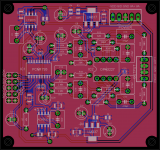
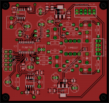
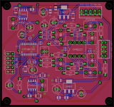
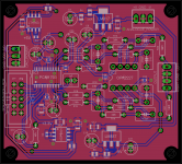
Hi all, just been designing a PCB for the TI DAC IC PCM1793. The datasheet specification is excellent and provided that spec can be met the DAC should offer exceptional performance at reasonable cost.
This design uses ultra low noise regulation for the analogue 5V rail, high PSRR 3.3V regulation for the digital section by a regulator stable with MLCC output capacitor. The Op-amp is one of the lowest noise types at modest cost with attractive specs all round (offset and input currents are important here). Regulated supply to the Op-amp is by LM317/337 pair set to +/-9V (easily enough to provide the full output this DAC is capable of).
The output filter/bal to SE converter is dimensioned to produce performance matching that in the datasheet, but using capacitor values available from the WIMA FKP2 range.
I hope that the layout can perform. I've tried to add local bypassing to each of the discrete 5V pins on the DAC, however I've not managed to return the bypass directly to the associated ground pin in all cases. Hopefully with the ground plane this is still sufficient? I believe the Vcom cap can be susceptible to noise; hence the smaller form factor film type being used here. Is there perhaps a benefit to bypassing it with a larger electro as well? The standard resistors in the filter circuit are to give flexibility in obtaining and matching the parts; the higher power rating may be welcome to reduce noise too.
A quartet of these may eventually be paired with my other board, the CS3318 volume controller:
CS3318 PCB Layout thread
Any input on optimising this design is welcome! Board costs are hopefully modest due to the small size (64x60mm).
Attachments

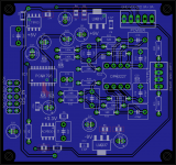
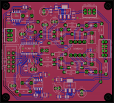
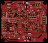
It is not possible to see on the pictures if you have vias close to the GND terminals of e.g. C25 and C29. I assume that there is a via here. Otherwise you will couple noise from the digital part into the analog part.
I would suggest to turn C25 (clockwise) and C29 (counterclockwise) by 90 degrees and connect the GND terminals directly to pins 8 and 9.
If you turn also C24 you can connect the GND directly to pin 19.
The 3.3V supply should probably be taken from C5 and not from pin 1 and 2 of the IC, but that is a minor thing.
I have only reviewed the design briefly. I would suggest to add via holes (if not already present) in a lot of places to connect the GND planes and minimize the loop lengths of decoupling paths.
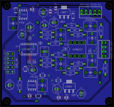
Your grounding is terrible.
On the bottom plane, ground has to travel all the way around the outside
of the board to get to inside.
On the top is not much better. Ground has to travel all the way around the LM317 and
the LM337 before getting to the inside.
On the bottom plane, ground has to travel all the way around the outside
of the board to get to inside.
On the top is not much better. Ground has to travel all the way around the LM317 and
the LM337 before getting to the inside.
Good input, some of it is quite glaring and I think I was a bit hasty posting the design, apologies.
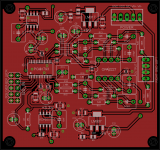
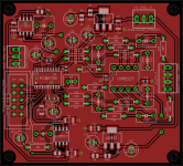
The subtle, but hopefully much improved Rev1 is attached. I have re-orientated the capacitors and joined them to their respective ground where possible. I've excluded part of the ground fill (under the IC) so that digital ground returns to C29 before being bonded to the main ground surface, this feels like the right thing to do? Most improvements to the ground are simply by placing the GND header pin on the inside rather than outside but I've considered the various return paths and moved some tracks and added a few vias to hopefully keep impedance low. There's many through-hole components with a grounded lead around so this bonds the planes together at many locations as well. My main concern now is the +9V feed trace to the op-amp since the bottom side is quite broken up around here too.
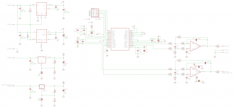
Some other details on the design, data is I2S 24bit, I could add a jumper to select 16bit as an alternative but every device I've seen now produces 24bit and just pads 16bit data streams. Mute is unused, I plan muting upstream of this, and Reset is a simple RC affair, the Reset input is Schmitt action so this is fine to do. The DAC IC may be fully shutdown by connecting S/D to GND.
The subtle, but hopefully much improved Rev1 is attached. I have re-orientated the capacitors and joined them to their respective ground where possible. I've excluded part of the ground fill (under the IC) so that digital ground returns to C29 before being bonded to the main ground surface, this feels like the right thing to do? Most improvements to the ground are simply by placing the GND header pin on the inside rather than outside but I've considered the various return paths and moved some tracks and added a few vias to hopefully keep impedance low. There's many through-hole components with a grounded lead around so this bonds the planes together at many locations as well. My main concern now is the +9V feed trace to the op-amp since the bottom side is quite broken up around here too.
Some other details on the design, data is I2S 24bit, I could add a jumper to select 16bit as an alternative but every device I've seen now produces 24bit and just pads 16bit data streams. Mute is unused, I plan muting upstream of this, and Reset is a simple RC affair, the Reset input is Schmitt action so this is fine to do. The DAC IC may be fully shutdown by connecting S/D to GND.
Attachments
The grounding is much improved.
I'll go through it in more detail when I have more time.
Just time for a quick look right now.
I'll go through it in more detail when I have more time.
Just time for a quick look right now.
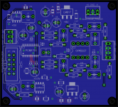
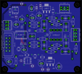
Look at the connection from C8, move R8,R9 route this track through the middle of these restistors. You can then move the traces from the bottom layer that go to and from R10, 11, 12, 13, 14 IC2 C14 to the top layer. Look around the board and do this in other places. You want as few traces on the bottom layer as possible, and any that are left route so they do not cut the ground plane. Then add stitching vias between the top GND copper pour (it is not a plane) any Caps and GND pins to this bottom plane.
I see what you're saying, to basically strip away as much as possible from the bottom and use it as the ground return 'plane'. I've tried this out in Revision 2 (attached). The bottom fill is now very open in the centre and vias link the top to the bottom where there are grounded components with no local through hole ground link.
Thanks!
Thanks!
Attachments
Looks a lot better, well done. That's what PCB designs about, the more you do the more you can see the routing as you place the components. And having only two layers to play with really taxes the brain.
Another tip, leave a design alone for a day or so after you finish it, don't look at it or think about it, then go back and check it, you will always find something that you wonder why you did it like that or some area you can improve.
Glad to help.
Another tip, leave a design alone for a day or so after you finish it, don't look at it or think about it, then go back and check it, you will always find something that you wonder why you did it like that or some area you can improve.
Glad to help.
Ditto what Marce said.
Suggestions:
* Move the power connector next to the I2S connector. That would reduce the length of the VDD traces.
* Eliminate the S/D signal. Its intended use is to turnoff unneeded regulators to save power while a device is in standby mode. I don’t see the need in your DAC. Mute is the proper signal to silence the DAC. Route MUTE to pin 10 of the I2S connector.
* Alternatively, route the DAC’s RESET signal to pin 10. Pulling RESET low has the same overall effect as shutting down the +5v and +3.3v regulators.
* Use a 6-pin power connector. Interleave VDD, VA+, and VA- with grounds and wire as twisted power/ground pairs.
* Every ground connection, including all SMDs, should have a dedicated via connecting the top and bottom ground pours. C9 has no via. Likewise pin 4 of the ADP3301. In other cases, such as C30, you rely on the ground of a nearby through-hole component. I prefer to overlap the via and the pad or connect the via to the pad with a short, no-clearance trace. That way, if sometime later I move the component, it is obvious the via has to move with it.
Just another remark:
I'd try to change routing of +3V3 to pins 26 and 28 (FMT 0 and 2). The trace from R7 to the IC cuts ground returns of I2S signals!
I'd try to change routing of +3V3 to pins 26 and 28 (FMT 0 and 2). The trace from R7 to the IC cuts ground returns of I2S signals!
Thanks for the suggestions!
I see what you mean about moving the connector, it would allow the incoming I2S a direct return to Ground and reduce the length of power traces. I'm probably thinking about this the wrong way, but if the power connector is located close to the digital section does this not effectively place the analogue components upstream of the digital ground noise and make them more susceptible to being influenced? I tended to imagine the analogue should be grounded close to the connector with digital upstream of it, in mixed signal boards. Either way, this is a receiver and digital switching currents should be small, but I'm keen to know the correct practice.
The shutdown does add a bit of slightly untidy wiring but the datasheet didn't specify whether Reset was a low-power mode. It usually is, when I've used Cirrus DACs this has been the case, but they specify it as such and quote a low-power current draw where this device doesn't. I'll be running 4 of these boards in a box so I'd like to be able to employ a low draw standby mode. Muting will be upstream on the still to be designed line driver board (probably based on THAT1646).
I think a separate Ground return for the Op-amp section is wise since this will come from a separate transformer. I'll use a centre tapped one though so the ground for +V and -V is shared regardless. It comes down to whether it is best to join the VDD and V+/V- grounds back at the power distribution board or on this board, the TI datasheet suggests probably leaving the supplies isolated from each other at distribution and allowing the connection through the board grounding, to reduce signal ground return lengths.
I did miss a couple of vias, noticed the ADP3301 one soon after I posted! Good tip to come back to the work later on marce!
curryman, yes, I think I will instead tie these pins to the local 5V since they are 5V tolerant inputs, this avoids the bottom side routing at all.
Thanks again!
Another short remark: why did you choose leaded Film caps for C1 and C4? According to ADP3301 datasheet traces should be kept as short as possible. Maybe use a 0805 (or 0603) 10nF COG here?
Hi, low leakage was the key parameter I picked up on for these, which the Polyprops are fantastic at. Noise pickup is a legitimate concern however but these are located quite close really, the board is tiny.
EDIT, I can make the trace to NR shorter on the left side of the ADP3301 though so will try this.
EDIT, I can make the trace to NR shorter on the left side of the ADP3301 though so will try this.
Last edited:
Ok, here's what I hope can be a final version!
The board now has separate DAC and analogue (buffer/filter) power headers. The respective grounds will return to two independent power supplies so the only join between grounds is through this board. I believe this is a good way to handle it?
Footprints for the WIMA capacitors have been updated to reflect exactly their dimensions. Also the input header footprint has been updated for an IDC header, it looks really big on this board!
Vias have been added everywhere they are required (I hope!)
My main concern now it how to correctly assemble 4 of these boards into a system where they share power supplies and unfortunately grounds will have to be tied together by the I2S source.
Attachments
Looks good, but I will also recommend that C1 and C4 are the wrong choice for their function, an 0603 next to the pins is the best option. I have done hundreds of boards with various LDO supplies (some board may have 22 separate supplies) and do a lot of power supply layouts for quite demanding applications (mill areo and medical) and have worked closely and been tutored by the apps engineers at both Ti and Linear (amongst others) and one of the first things I was taught was:
Place all components connected to high impedance pin should be placed first to minimise lead length, FB (Feed back pin taking priority).
This capacitor is acting as a decoupling capacitor for the internal voltage reference and as such should follow all the rules for bypass capacitors, a low inductance device (SMD) and short leads. Your capacitor choice breaks both these rules and you would be much better using an 0603 COG capacitor next to the pins, the pitch between pins 3 and 4 is 1.27mm, an 0603 capacitor is 1.60mm long, this placed adjacent to the pins will give short trace length and thus the minimum inductance, most important for decoupling capacitors. Your solution is more likely do nothing for the noise or worse actually add noise.
For the Linear regulator have a look at the evaluation board:
LT1763 - 500mA, Low Noise, LDO Micropower Regulators - Linear Technology
Not the position of C2. The design file download has a set of PDFs of the layout.
When doing designs with any sort of power supply both myself and the engineers working on the design use the manufacturers provided layout as a guide, and do not deviate from this design.
The routing to C! is particularly bad, one leg going to a star point then back to the pin.
Sorry if I seem over critical but with any PSU the detail is critical to a optimum layout and thus performance and currently these two caps are incorrect.
Marc.
Well I would be foolish to ignore this advice now that two of you have pointed it out to me! To be fair, the WIMA footprint is even bigger than I first realised and noise pick-up could likely occur within the cap as well as the PCB trace.
I suppose it's like the 22uF bypass on the LM317/337 pair, here we are forced to use such a large value because the load impedance is a mere 2k. The low voltage regs can use a smaller and lower leakage cap, 10nF is recommended, but the impedance would need to be 4.4M to match the break frequency, and that is substantial.
They will be changed to C0G, and I will place them directly between the IC output and the NR pin, not at the bulk output capacitance.
I inkjet printed the board earlier too and feel the mounting screws are a tad close to the board layout so this might get adjusted. Otherwise the footprints all seemed correct.
Thanks again!
Not much to say now, capacitors are C0G 10nF located close to the regs and clearance around the mounting points has been increased 🙂
Still unsure how grounding multiple boards will work out since multiple ground returns become unavoidable when sharing an I2S source (likely MiniDSP USB streamer). Unless isolators (GMR or similar) are added to this board, but I am unconvinced about their preservation of low jitter performance.
I have also not prepared a board for manufacture yet, some board houses appear to accept Eagle files directly but perhaps it's always best to use Gerber files. On the PDF printout I did the small copper pour mask area came out as solid fill rather than exclusion area so I'm not sure if that will present a problem for manufacture.
Attachments
 Those are what you call short traces🙂
If you haven't got it already, GCPrevue is a free Gerber viewer.
Hi Dr_EM,
Great job, I wish I could get mine done.
I am far from an expert but I will offer a few suggestions anyway. 🙂
Great job, I wish I could get mine done.
I am far from an expert but I will offer a few suggestions anyway. 🙂
- You may have a problem with your gerbers if you don't use vector fonts on your board.
- C10 and C12 could be connected more like your LM317.
- You have made the position of the components of the output stage very symmetrical except for R15 and R16. Move them down a little. Likewise, line up R20 and R21.
- Label R12 almost touches C14.
- There is a 90 degree bend under R9.
- Are your resistors 7.5 or 10 mm spacing? 7.5 mm is a squeeze for some resistors. They will fit but look a little ugly.
Thanks! I have grabbed that viewer, it looks more promising than the other free one I tried.
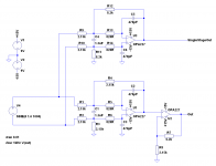
Greg, I have gone ahead with most of those changes, however I was just revising the resistor footprints (I too had noticed they required a very tight bend when testing on the printout) when I remembered I wanted a hotter output from this ideally, so was going to increase R12,13,14,19. The higher output level should help maintain the SNR as the signal passes through analogue volume control and balanced line driver stages (which have excellent performance but should operate at >+12dBu to maintain a 113dB theoretical SNR). At the power amplifier end, either low-gain circuits or attenuating line receivers (Jensen make some beautiful transformers for this, not affordable for 6 channels mind!) will scale the signal for clipping at around -6dBFS input.
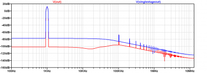
When checking the calculated gain was correct in simulation I noticed what frankly appears to be unacceptable THD+N, mostly noise, on the FFT. This is using an official OPA227 model (single version of 2227) however similar results were obtained with any op-amp I tried.
The noise floor appears to increase beyond the gain, thereby worsening the SNR as gain and output are increased. However, by using a unity gain filter followed by an independent gain stage, far better results are obtained. I'm wondering if this is a case of making a single op-amp do too much by asking it for reasonable gain as well (to put it in very inexact terms!) or whether I'm merely seeing a quirk of simulation (simulation is using no compression and alternative solver)? Even with the previous gain of 5.2dB the noise floor was being, apparently, compromised.
Any insight here appreciated, I'll happily add a second op-amp if this simulation is accurate!
Greg, I have gone ahead with most of those changes, however I was just revising the resistor footprints (I too had noticed they required a very tight bend when testing on the printout) when I remembered I wanted a hotter output from this ideally, so was going to increase R12,13,14,19. The higher output level should help maintain the SNR as the signal passes through analogue volume control and balanced line driver stages (which have excellent performance but should operate at >+12dBu to maintain a 113dB theoretical SNR). At the power amplifier end, either low-gain circuits or attenuating line receivers (Jensen make some beautiful transformers for this, not affordable for 6 channels mind!) will scale the signal for clipping at around -6dBFS input.
When checking the calculated gain was correct in simulation I noticed what frankly appears to be unacceptable THD+N, mostly noise, on the FFT. This is using an official OPA227 model (single version of 2227) however similar results were obtained with any op-amp I tried.
The noise floor appears to increase beyond the gain, thereby worsening the SNR as gain and output are increased. However, by using a unity gain filter followed by an independent gain stage, far better results are obtained. I'm wondering if this is a case of making a single op-amp do too much by asking it for reasonable gain as well (to put it in very inexact terms!) or whether I'm merely seeing a quirk of simulation (simulation is using no compression and alternative solver)? Even with the previous gain of 5.2dB the noise floor was being, apparently, compromised.
Any insight here appreciated, I'll happily add a second op-amp if this simulation is accurate!
Attachments
- Status
- Not open for further replies.
- Home
- Source & Line
- Digital Source
- PCM1793 PCB Layout