I am not sure if this is the correct sub forum for this, but I am sure there are people here who could help on this.
So I picked up a piece of non-working gear from ebay to do more troubleshooting and learning how to fix more things.
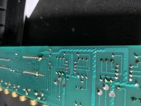
The picture attached is from a B&K CS117 and the problem they listed is it kept popping fuses. So the trace that has all the bubbles in it is one of the main ground traces on this PCB.
Now my question is; if it was yours, and you wanted to keep the item, would you gently cut the top layer, check the trace itself and say it was in the shape as the top; remove and replace it?
If you replaced the trace, where would you locate that and also what would you use to then cover it.
Now I know I need to find out why this was caused, but I do not want to cover that here, just what your thoughts on a repair.
Thanks, James
So I picked up a piece of non-working gear from ebay to do more troubleshooting and learning how to fix more things.
The picture attached is from a B&K CS117 and the problem they listed is it kept popping fuses. So the trace that has all the bubbles in it is one of the main ground traces on this PCB.
Now my question is; if it was yours, and you wanted to keep the item, would you gently cut the top layer, check the trace itself and say it was in the shape as the top; remove and replace it?
If you replaced the trace, where would you locate that and also what would you use to then cover it.
Now I know I need to find out why this was caused, but I do not want to cover that here, just what your thoughts on a repair.
Thanks, James
Attachments
It looks to me like a thick plating was used on the trace before solder mask was applied. This is sometimes done to reduce resistance in high current traces.
Thank you very much for your reply.
So you have seen traces with bubbling under a “normal” circumstance?
So you have seen traces with bubbling under a “normal” circumstance?
This is common in computer SMPS, the solder is added to take higher current than what can be handled by the foil alone.
Just wavy, not important.
Your fault is elsewhere.
Use a dim bulb tester, after checking for obvious shorts or shorted components.
Read up here.
Get the schematic, find and fix the fault.
Enjoy the music after that.
Just wavy, not important.
Your fault is elsewhere.
Use a dim bulb tester, after checking for obvious shorts or shorted components.
Read up here.
Get the schematic, find and fix the fault.
Enjoy the music after that.
Well, right now I am still in the process of cleaning up the two PCB'S that make up this unit. I cannot stand having resin or flux on the solder pads, drives me crazy.
As for the schematic, there is not one to be found anywhere, so I am just going to need to just draw out the connections from point A to B and such. I can see where everything is going since I can see through the PCB.
As for the schematic, there is not one to be found anywhere, so I am just going to need to just draw out the connections from point A to B and such. I can see where everything is going since I can see through the PCB.
Find out what is the output stage.
It is rare for amplifiers to have unique circuits.
Most have bought out components.
So it is quite common for Kenwood and B&O to use the same circuit.
You pay a lot more for B&O, and its fancy dress housing.And sometimes find very bad capacitors inside.
Blown fuses means power supply and output stage, then on from there.
Yes, cleaning for measurement device is possibly needed too, but usually it is not the problem of popping fuses.Well, right now I am still in the process of cleaning up the two PCB'S that make up this unit. I cannot stand having resin or flux on the solder pads, drives me crazy.
As for the schematic, there is not one to be found anywhere, so I am just going to need to just draw out the connections from point A to B and such. I can see where everything is going since I can see through the PCB.
I would start an investigation with a power supply. First with an unregulated, then I'll go to regulated ones.
PCB traces on the photo look fine. It it is a bubble then it can be whipped trough but I'm 99% sure it is a solder added and painted then.
Last edited:
I agree with you that a dirty board (per se) would not be a probable cause; but for me; I like to start with a clean device, which means I will be touching all the components and by a VERY small chance run across something loose.
Not a lot of time to trouble shoot in the next few days as I am doing a lot of the "classes" in the Industry Tech Days from All About Circuits.
Not a lot of time to trouble shoot in the next few days as I am doing a lot of the "classes" in the Industry Tech Days from All About Circuits.
It looks too consistent to be bubbling.
Sometimes they run solder along the track to bulk it up.
Or someone just did a poor job of HASL or maybe deliberate ?
Sometimes they run solder along the track to bulk it up.
Or someone just did a poor job of HASL or maybe deliberate ?
I used to see that kind of zigzagging solder ridges all the time in the 80´s, particularly in Gallien Krueger amplifiers and many effects pedals.
Suppose it fell out of favour (at least as shown) because it involves an extra step of applying solder mask or protective coating *after* board has been through wave soldering machine, a PITA.
Suppose it fell out of favour (at least as shown) because it involves an extra step of applying solder mask or protective coating *after* board has been through wave soldering machine, a PITA.
Ancient through-hole PCBs used wave soldering, where the board passes over a standing-wave in molten solder to solder the through-hole components - I think this effect is when the PCB is pre-tinned using the same process and excess solder adheres to the traces before solder-mask is applied. As far as I know its not deliberate and was viewed as benign back in the day.The picture attached is from a B&K CS117 and the problem they listed is it kept popping fuses. So the trace that has all the bubbles in it is one of the main ground traces on this PCB.
Modern PCB fab uses electroplating or HASL (hot air solder levelling) for tinning the traces to avoid such lumps. Unless they are shorting things out or peeling off the solder-mask they are benign. Modern fine-pitch SMT components would tombstone or get shorted if excess solder existed on traces like this and moved around during reflow, which means you don't see this lumpiness any more, or that's my best guess at least.
- Home
- Design & Build
- Parts
- PCB Trace