
Very interesting, are some papers about this phenomenon existing?
I don't know, since I never really looked for anything. Another note, This happened over 20 years ago. I'm not sure if it is an issue with today's material, and probably not a problem for a board made by a reputable PCB house.
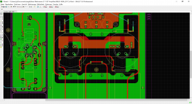
A PC Ft. Lauderdale board manufacturer (Davco printed circuits) was shut down by the EPA in the 1980's. Some dumpster diving netted me about 100 pounds of double sided .062 G-10. I'm still using that same batch of material for my test boards.
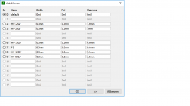
Creepage calculator treat Vdc equal to Vrms..
If you do not get actual ARCing, or a tall-spike waveform, most of the effects of leakage will be related to the "average" voltage not the peak.
RMS is not Average but all this is so approximate that a 10% (Sine) difference is unimportant-- we take at least 2:1 safety margin, hopefully more.
... we take at least 2:1 safety margin, hopefully more.
Such a margin is encoded in a standard like IEC 60950, or are you saying that we should at least double its recommendations?
Thanks,
Jeff.
I have come across instances of G10 material being leaky. We once even had to send a whole batch back to the supplier.
- Status
- Not open for further replies.