Hi,
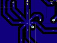
I've routed a PCB for the aikido power supply.
+B is around 300V. I used an online pcb trace
calculator and it shows around 200mil clearance.
The only reason I would need to use the clearance
is if I fill in the rest of the pcb with copper(no net).
Is it better just to have the traces without the copper fill?
Thanks.
Attachments
It's a little complicated... it depends on environmental conditions, and if your PCB has solder mask on it.
Look at IPC standard 2221, table 6-1. I found a copy here:
http://www.the-bao.de/divers/ipc2221.pdf
"Uncoated" (class B2) means no solder mask. Spacing requirements s are much larger without it. This shows 2.5mm (0.1") for 301-500V.
Add solder mask (class B4) and the spacing drops to 0.8mm (0.032"). This is more reasonable for most designs.
I usually use between 30 and 40 mil spacing for tube PCBs (with soldermask).
Pete
thanks Pete!
that's a very useful document.
My clearance right now is .15" so I should be okay.
Do you use any copper fill on your tube pcb's or just
just the traces?
I've read it's good have have copper between traces to help reduce noise. Yet I'm not sure if this still applies to High Tube voltages.
that's a very useful document.
My clearance right now is .15" so I should be okay.
Do you use any copper fill on your tube pcb's or just
just the traces?
I've read it's good have have copper between traces to help reduce noise. Yet I'm not sure if this still applies to High Tube voltages.
Tubes are inherently very high impedance devices. Stray capacitance can have negative effects on stability and frequency response. The magnitude of these effects are highly circuit and layout dependent. The worst case is a grid circuit trace that has ground on the other side
- Status
- Not open for further replies.