Greetings,
I'm thinking of building an ESL with Pcb as a stator, does anyone have a recomandation or some rules I have to follow ?
I've included a "doodle" how I would do it. The Gaps are spaced 2mm apart and the board outline is 200mm x 100mm. The horizontal white line is just an axis on which you can rotate, it's not part of the board. If you zoom in you can see the copper traces under the soldermask.
I haven't included any segmentation yet, it's just to get some advice ...
Attachments
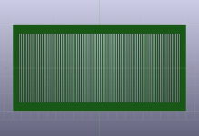
ita a bit to much open area vs copper. and using such long slots, will make it flimsy. maybe need some horizontal left over pcb as well every few cm
Hi,
soldermasks alone could be insufficient for our application, as their flashover voltage isn't high enough, resü. the thickness too low.
https://www.peters.de/en/home offer special pcb coatings and protective laquers that build up thick enough layers.
A nice feature of these special coatings is, that they form a soft rounded surface towards the hole edges, without getting into the hole itself, possibly closing it.
You must also think about which side shall point to the membrane and which one to the outside.
With a afore mentioned laquer coating the PCB side should point outwards and the copper and laquer layer to the membrane.
jauu
Calvin
Hi guys,
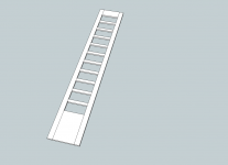
Back at that time I was thinking of placing these in a frame as in the picture, the thickness of the PCB is 1.6mm, I guess (hope) that's thick enough when put in a frame ?
If one puts the copper + soldermask layer to the outside and the pcb to the membrane, would this still not be enough for flashovers ?
I must say that I simply got inspired by a picture of an ESL by Sanders ...
Thanks for your help
Attachments
Hi,
the PCB material can withstand high voltages, so You'd be safe in this regard ... in fact I'd rather choose thinner material like 0.5mm to keep the required drive voltages low .... but/and.....
- You should protect the panel from getting touched by hand ..... You could get zapped
A safer method would be to use one of the afore mentioned coatings towards the inside, or to have a PCB manufactured with 1.5mm PrePreg to the outside and 0.5mm to the inside and the copper core layer in between.
- You should consider the shape and site of the openings in the PCB.
With rather small holes of say 3mm diameter or less the holes form kind of BR-port and reduce the upper bandwidth limit.
Here lower sheet thickness or larger hole diameters would help.
With long slots its probabely no issue .
In any case You'll need braces or other mechanical means to stiffen the PCB.
When designing the conductor pattern and isolating layer (soldermask) keep in mind that the copper layer be recessed a bit from the hole edges so that it is covered by the isolating layer in fullness.
jauu
Calvin
- Status
- Not open for further replies.