Hi all,
Are there any sites that tell you how to draw your own PCB layouts? I mean some principles or basic guidelines. We have software to do it but I nevertheless would like to read stuff dealing with this. Thanks.
Vivek
Are there any sites that tell you how to draw your own PCB layouts? I mean some principles or basic guidelines. We have software to do it but I nevertheless would like to read stuff dealing with this. Thanks.
Vivek
have a look at www.cadsoft.de and follow the guided tour
Best regards,
HB.
EDIT: also look at: http://www.terrypin.dial.pipex.com/ECADList.html
Best regards,
HB.
EDIT: also look at: http://www.terrypin.dial.pipex.com/ECADList.html
Still some mystery
The mystery is that after a couple of experiences using a PCM layout program with or without an autorouter, my layouts, though functional seem convluted and overly complex. That is in comparrison to boards of similar complexity (or lack of complexity) done by folks with more experience.
The key seems to be the placement of the components. Some locations are dictated my the need to be near the board edge (terminal blocks) components requiring off-board heatsinking). I try to place related compones is fairly close priximity, but it seems like doing that with one part of the cicuit frequently makes another section more complex. Of course, limiting myself to a single sided board makes routing tougher.
If anyone knows of a book or guidelines on the topology of board layout, particularly how to place the components with the aim of getting simpler traces, that would be helpful.
it really is a matter of cutting and pasting. I lay the stuff out on grid paper (1/10 or 1/4 inch) and move the actual components around. even then I prototype a board by hand and check to make sure that there is enough clearance etc. I then go into my layout program.
i use Ultiboard which has auto-routing, but i almost always "route-by-net". instead of ripping up the entire design, you can eliminate traces which look like they are going to be problematic as soon as they are laid down. Ultiboard also allows you to move traces as close to an adjacent trace as possible under your design rules and this helps make things look better. Ultiboard's support is sometimes lacking, and if you need a new install code on a weekend you're screwed.
http://www.expresspcb.com/ExpressPCBHtm/Tips.htm has some hints.
if in NYC the McGraw Hill bookstore has a rack of books on PCB design -- you can go in there and browse (you don't have to buy!)
PCB Design
Hi Vivek,
I use Boardmaker.
A few hints:
Resistors, capacitors can jump a track without making use of a jumperwire.
Try to jigsaw puzzle a bit with the parts.
Best have all IC's pointing one direction to avoid confusion.
Don't place parts to close to each other: you need space for tracks and surrounding components. Don't get yourself locked up in a tight corner.
Try thinking in advance: if I move or turn this part what will happen?: shorter connections etc.
Practice yields better results!
Tracks can run under IC's, transistors etc. I prefer NOT to run tracks between pins of IC's.
As a example if you have a FET oscillator followed by a AD8561 comparator it seems logical to place the FET at the left side of the comparator as pin3 is connected to the FET.
However if you are using a SMT AD8561 placed at the solder side of the PCB I woud place the FET at the right side. (I don't make double sided PCB's.)
Hope this helps.😎
Hi,
I use Eagle and I find it difficult to make single sided boards using the autorouter. Double sided boards are no problem but I prefer single sided boards.
Elso, thanks for the tips and thanks to Jack and Sam.
Vivek
I use Eagle and I find it difficult to make single sided boards using the autorouter. Double sided boards are no problem but I prefer single sided boards.
Elso, thanks for the tips and thanks to Jack and Sam.
Vivek
Eagle tip
Vivek,
Here's my top tip for PCB layout, hope it's of use!
First, never use the autoroute for analogue work, except for very quick and dirty proof-of-principles.
The autorouter will always produce a poor layout, with no consideration for current paths etc.
Do use it though to get an idea whether your coomponent placement will be routable - you can examine the autorouted results, look for obvious problem areas, and shift things around accordingly.
Once happy with postioning, rip up the autorouted tracks and route manually - it's a whole load more fun, will give better results, and you'll have a much more elegant result at the end.
All Elso's tips are spot on - think about how resistors, diodes etc. can jump tracks for example and you'll soon get the hang of it.
I often spend more time on board design than circuit design, as poor implementation can ruin an otherwise excellent design.
Andy.
Hello Vivek!
I agree with Elso.
The basics of designing a PCB is very important. Nowdays easy, because the design softwares have many options, and you can play with it, make undo, etc.
Earlier it was much more difficult, because you have to draw on the paper, couple of times, because every time it came new idea, how it is better.
You have to know well the schematic and how is it working, because on that way you know, that what the part is doing in the circuit, what you place at the moment.
After it you can decide to use short signal path or longer, or take care about power supplying, power traces (eg. digital circuits vs analog circuits).
But it gives a good practice: you learn, how to place the components, on which angle, which position. With SW you can play a lot, and much more easier.
But in the beginning I recommend to you to play a lot: it gives practice, and later on you can try a more complicated circuits also.
I use Protel, and I am satisfied with it. Usually I am not use the autoroute function, I make the traces ownself.
This is because the autoroute options not every time make the traces on the way, how I want them, and the circuits, what I design are not so complicated.
Usually you can "play" first the component placement as much as possible. If you have placed the components not just for nice looking point of view, but also for short signal path, the route of the traces will came in your mind meantime.
So, when you place the components, it is in your mind where the traces will go.
If you design more complete circuits, it is possible to use autoroute functions, but partly you can route by hand the most important traces (eg. signal path, or power tracks, depend on your priority).
What I do usually:
1. Draw the schematic in schematic editor
2. Transform it to PCB editor
3. Place the components manually (it takes a time to achieve the best placement for you)
4. Route the tracks (it takes time also, because many times you can see, the the component can be on an another place, which is best, see point 3.)
5. Print the film (by inkjet or laser printer) I prefer inkjet, because one film is enough for photo.
6. Photo and enthcing
7. Drill
8. Lacking
9. PCB ready
This is mainly for single sided boards, because it is easy to make at home.
For more complicated boards better to use Gerber or CAM export, and send the files to PCB manufacturer to make it (-> expensive!)
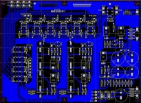
Here is an simple example, where you can see that first the components was placed carefully, and later on the traces was routed.
BR,
Milan
I agree with Elso.
The basics of designing a PCB is very important. Nowdays easy, because the design softwares have many options, and you can play with it, make undo, etc.
Earlier it was much more difficult, because you have to draw on the paper, couple of times, because every time it came new idea, how it is better.
You have to know well the schematic and how is it working, because on that way you know, that what the part is doing in the circuit, what you place at the moment.
After it you can decide to use short signal path or longer, or take care about power supplying, power traces (eg. digital circuits vs analog circuits).
But it gives a good practice: you learn, how to place the components, on which angle, which position. With SW you can play a lot, and much more easier.
But in the beginning I recommend to you to play a lot: it gives practice, and later on you can try a more complicated circuits also.
I use Protel, and I am satisfied with it. Usually I am not use the autoroute function, I make the traces ownself.
This is because the autoroute options not every time make the traces on the way, how I want them, and the circuits, what I design are not so complicated.
Usually you can "play" first the component placement as much as possible. If you have placed the components not just for nice looking point of view, but also for short signal path, the route of the traces will came in your mind meantime.
So, when you place the components, it is in your mind where the traces will go.
If you design more complete circuits, it is possible to use autoroute functions, but partly you can route by hand the most important traces (eg. signal path, or power tracks, depend on your priority).
What I do usually:
1. Draw the schematic in schematic editor
2. Transform it to PCB editor
3. Place the components manually (it takes a time to achieve the best placement for you)
4. Route the tracks (it takes time also, because many times you can see, the the component can be on an another place, which is best, see point 3.)
5. Print the film (by inkjet or laser printer) I prefer inkjet, because one film is enough for photo.
6. Photo and enthcing
7. Drill
8. Lacking
9. PCB ready
This is mainly for single sided boards, because it is easy to make at home.
For more complicated boards better to use Gerber or CAM export, and send the files to PCB manufacturer to make it (-> expensive!)
Here is an simple example, where you can see that first the components was placed carefully, and later on the traces was routed.
BR,
Milan
Attachments
I forgot some things:
When you design the circuit be carefully with your component sizes.
So first, I recommend to buy first all the components, and later on design the PCB.
On that way you can eliminate some very aggravating problems.
Eg. the PCB is ready, and the component is not fit to the place 😡
I had some times this problem, beacuse I had only 90% of the components, and the PCB was ready. But, because of the components availability, I got different size components to some positions.
So, be carefully with it, and design the PCB to the components.
Hey, this thread is getting very informative.
As I understand it, the layout for say a power amplifier can affect the sound quality. That obviously calls for some practice.
The software that produces the board layout just lines up all res, caps etc in a line, so I hope it is okay to shift them. I thought the software does the optimum placement and it would not be wise to shift the components around.
Mpopovics, Andy, great help.😀
hi,
i tried to design some boards with the IVEX, and i found out that it is not easy at all.
infact it is very problematic and risky, at least to me.
then i saw the layouts from the PCB-DESIGN (http://web.vip.hr/pcb-design.vip) , unbeliveable... i never saw something like that before, not only that the layouts are well done, but they are also very simetric, infact they are simetric, even if the circuit diagram is far from that.
i talked to PCB-DESIGN and ask what software they used for designing the Aleph boards. the answer was PROTEL and TANGO, the all boards are SINGLE SIDED and that there is not used any help from autoruter !!!
now i see the mpopovics work, very good, and again it is done with the PROTEL, and also without autorute.
how that it is possible ?
am i missing something or ...
Attachments

Ivex
I just want to confirm your comment about IVEX. It can be made to work but if you are easily angered or frustrated it is best avoided. Amoung otherthings, it crashes under Win98 on a regular basis. Under WinXP, you have to download and unofficial patch and turn off any any-virus software. It's only virtue that I see is that it is cheap.
I've downloaded a pin-limited version of Vutrax, appearently a full professional level product out of the UK. I'm still working my way through the tutorials which are very extensive, which go beyond just documentiong what all the menu choices are but include quite a bit of practicle procedural device. So far I'm fairly impressed. My only dissapointment is that their library of discrete devices does not include all that I would like, so I expect to have to create about half symbol/footprint combinations I use.
chorei said:hi,
i tried to design some boards with the IVEX, and i found out that it is not easy at all.
infact it is very problematic and risky, at least to me.
.
I just want to confirm your comment about IVEX. It can be made to work but if you are easily angered or frustrated it is best avoided. Amoung otherthings, it crashes under Win98 on a regular basis. Under WinXP, you have to download and unofficial patch and turn off any any-virus software. It's only virtue that I see is that it is cheap.
I've downloaded a pin-limited version of Vutrax, appearently a full professional level product out of the UK. I'm still working my way through the tutorials which are very extensive, which go beyond just documentiong what all the menu choices are but include quite a bit of practicle procedural device. So far I'm fairly impressed. My only dissapointment is that their library of discrete devices does not include all that I would like, so I expect to have to create about half symbol/footprint combinations I use.
- Status
- Not open for further replies.
- Home
- General Interest
- Everything Else
- PCB layout sites