Hi,
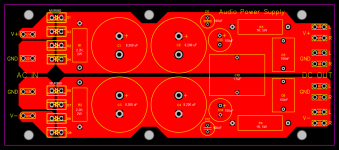
Wondering if anyone would like to check out my PCB layout for a gainclone power supply, based on CarlosFM's snubberized PSU schematic.
I'll be running two channels of LM3886 chip amps from this single supply with a 18-0-18 300VA toroid transfomer, and wiring it to the amps like the diagram below.
The PCB has a full ground plane and power plane for each rail. Will this work OK?
One question I had was whether or not to separate the ground planes for each rail. I've heard conflicting answers. Should they be connected?
Please comment, critique, and tell me what's wrong with my design. This is my first power supply, so I'm sure something could be improved...
Attachments
Hi,
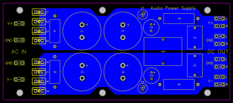
I would suggest to drop the CarlosFM's PSU design and implement the CRC transformer snubber before the rectifiers and make your PSU a CRC topology with a small value R. You also have wrong labeling of the input connectors: AC side does not have plus/minus and GND; in your current implementation you also do not have GND on the DC output side since GND in dual polarity supply is common to both rails.
Looking at your LM3886 PCB design idea in your other thread I think you should have one common GND plane on the PSU PCB. Your current (separate supplies) design is more suited for the chipamp.com kit where the common GND is implemented on the amplifier board.
In any case you leave too much space for the film capacitors, you can easily use RM5 type here or better skip them all since they do not improve anything because they are too far from the point of load. You also have an unnecessarily large PCB outline which will eat the space inside of your chassis. I would also make the mount holes on the DC output side inline with the connectors. You would not want to bend the PCB each time you insert the connectors.
Regards,
Oleg
the input from the transformer is AC
do not use "+" nor "-" symbols.
I suggets you remove the GND symbols.
Try using AC1, AC2, AC3, AC4 for the four input terminals.
Use double sided pads for ¼" spade terminals. Single sided are at risk of pulling off.
There may be an advantage to connect the Zero Volt planes at the output end.
I agree with Oleg, drop the Carlos and adopt a correctly snubbered transformer with a conventional PSU.
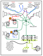
Don't use third "wiring" diagram. It uses many single wire connections. This will suffer emi issues.
Have a look at Bonsai's amplifier wiring pdf.
Have a look at Bonsai's amplifier wiring pdf.
Can you confirm your transformer is 18-0-18 VAC and not 0-18V 0-18V. If your transformer has a single 0V (center-tap) then your PSU design will not work.
Are you going to manufacture the board yourself? If so, consider that the through holes are not plated, this makes it impossible to solder the capacitors from the top side.
Are you going to manufacture the board yourself? If so, consider that the through holes are not plated, this makes it impossible to solder the capacitors from the top side.
Last edited:
Can you confirm your transformer is 18-0-18 VAC and not 0-18V 0-18V. If your transformer has a single 0V (center-tap) then your PSU design will not work.
Yes, sorry the transformer is 0-18V 0-18V not 18-0-18...
Are you going to manufacture the board yourself? If so, consider that the through holes are not plated, this makes it impossible to solder the capacitors from the top side.
I'm going to send the eagle files to a manufacturer since I don't have any experience using the toner transfer method
Hi,
I would suggest to drop the CarlosFM's PSU design and implement the CRC transformer snubber before the rectifiers and make your PSU a CRC topology with a small value R. You also have wrong labeling of the input connectors: AC side does not have plus/minus and GND; in your current implementation you also do not have GND on the DC output side since GND in dual polarity supply is common to both rails.
Looking at your LM3886 PCB design idea in your other thread I think you should have one common GND plane on the PSU PCB. Your current (separate supplies) design is more suited for the chipamp.com kit where the common GND is implemented on the amplifier board.
In any case you leave too much space for the film capacitors, you can easily use RM5 type here or better skip them all since they do not improve anything because they are too far from the point of load. You also have an unnecessarily large PCB outline which will eat the space inside of your chassis. I would also make the mount holes on the DC output side inline with the connectors. You would not want to bend the PCB each time you insert the connectors.
Regards,
Oleg
Thanks! That's all good to know. I'll try to implement as much of that as I can. The CRC transformer snubber looks good but unfortunately I don't have access to an oscilloscope to find the right RC values. Any other options?
By the way, what's an RM5 capacitor? Couldn't find much on google, is that a rating or a type of substrate?
Also good point about the mounting holes.
Last edited:
the input from the transformer is AC
do not use "+" nor "-" symbols.
I suggets you remove the GND symbols.
Try using AC1, AC2, AC3, AC4 for the four input terminals.
Use double sided pads for ¼" spade terminals. Single sided are at risk of pulling off.
There may be an advantage to connect the Zero Volt planes at the output end.
I agree with Oleg, drop the Carlos and adopt a correctly snubbered transformer with a conventional PSU.
Ok got it. I'm working on a version 2 now

RM5 (Rastermaß) is the leads pitch (spacing) of 5mm or ~0.2 inch. I guess it is a not so common German nomenclature... my bad.
- Status
- Not open for further replies.
- Home
- Amplifiers
- Power Supplies
- PCB Layout questions for PSU with ground/power planes