I've designed many complex digital layouts but never anything analogue and certainly not valve.
I've created a PCB layout for the RH84 design amplifier and would appreciate comments on the layout. I've attached two versions: the basic layout, and one with a ground plane copper flood - something that is routine for digital.
The layout is single sided with no jumpers needed. The heaters are not included as I would intend to wire these separately with twisted paired wire routed away from the PCB. The PCB size is 100x200mm which is the size of the blanks I happen to have available. All HT traces have a separation of at least 2.5mm from any other trace which should be good for 315VDC without solder resist.
All comments appreciated
Image1 — ImgBB
Image2 — ImgBB
Last edited:
Are you going to mount the PC board to a metal chassis? If so I don't think you need to worry about the filled plane.
You have made a very good choice to keep the heaters off the PC board. I just did some troubleshooting for a well known preamp kit that is all built on a PC board. The heaters were moderately filtered DC and the negative leg flowed through the ground plane. Disconnecting all of that and running AC twisted pair off the board dropped the noise floor 20dB.
One thing that does jump out is that you have all your mounting points on the outside corners. When you push the tubes into the sockets, the board will tend to flex in the middle. One more mounting support right in the center of the board would make a big difference.
I think this is very good.
I've designed many PCB with tubes and I once had issues with trace too close.
I now set a minimal of 2 mm between HV trace and the rest. Yours are 2.5 mm is perfect.
I don't see your heater traces.You have to be careful with those, and make sure they are away from everything grid related. I usually make them run on the external of the board, sometimes on top of each other on each copper sides, and when needed, cut other trace at a 90 degree angle on the other copper layer.
I hope it helps
Brice.
One thing that does jump out is that you have all your mounting points on the outside corners. When you push the tubes into the sockets, the board will tend to flex in the middle.
Good point,
If tube sockets have 2 flanges w/ holes, you could tie those to mounting plane w/ offsets.
Thanks all. Will definitely include a central support hole. As per original posting heaters will be separately wired with off-board twisted pairs. Next job a power supply PCB.
Very nice professional work.
1) I would suggest making ground plane taking less space to avoid extra parasitic capacitance between PCB top and bottom layers.
2) You will need standoffs to keep long heater wiring in place.
3) BIAS wiring can be made with ordinary wires to avoid long tracks with unnecessary complex routing on PCB.
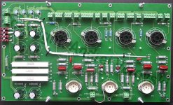
Photos of PCB and assembled prototype on test bench attached.
1) I would suggest making ground plane taking less space to avoid extra parasitic capacitance between PCB top and bottom layers.
2) You will need standoffs to keep long heater wiring in place.
3) BIAS wiring can be made with ordinary wires to avoid long tracks with unnecessary complex routing on PCB.
Photos of PCB and assembled prototype on test bench attached.
Attachments
Last edited:
One thing that does jump out is that you have all your mounting points on the outside corners. When you push the tubes into the sockets, the board will tend to flex in the middle. One more mounting support right in the center of the board would make a big difference.
Make more mounting holes on the edge, like on my previous post picts, and there will be no flex problem. PCB needs to be 2mm thickness of course.
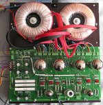
Power tubes should imho be mounted in "chassies-type sockets" screwed to chassies or
of needed in the board. Then short wires connected to sockets to the board.
This as powertubes will get very hot, and this might degrade the board, also the
sockets themself migh need replacements, replacing sockets in a partially
degraded boards is risky.
of needed in the board. Then short wires connected to sockets to the board.
This as powertubes will get very hot, and this might degrade the board, also the
sockets themself migh need replacements, replacing sockets in a partially
degraded boards is risky.
of needed in the board. Then short wires connected to sockets to the board.
This as powertubes will get very hot, and this might degrade the board
There are teflon rings between sockets and PCB, its not visible on the photo.
BTW, in the future, I decided to chassis mount socket with metal auxiliary rings, so sockets may become easier to replace.
I've designed many complex digital layouts but never anything analogue and certainly not valve.
I've created a PCB layout for the RH84 design amplifier and would appreciate comments on the layout. I've attached two versions: the basic layout, and one with a ground plane copper flood - something that is routine for digital.
The layout is single sided with no jumpers needed. The heaters are not included as I would intend to wire these separately with twisted paired wire routed away from the PCB. The PCB size is 100x200mm which is the size of the blanks I happen to have available. All HT traces have a separation of at least 2.5mm from any other trace which should be good for 315VDC without solder resist.
All comments appreciated
Image1 — ImgBB
Image2 — ImgBB
If you shove some parts slightly you can also flood the now-open areas at the right side of the 2nd board.
Another point is the grounding of the plane. If I see it right, it is really a ground current plane. That means there are all kinds of currents running through it, uncontrolled. That may lead to noise and hum.
The preferred way would be to run your ground traces for best practice like a star ground, and ground your plane in only one spot, preferably at the input signal ground. To avoid your CAD system to indiscriminately connect all grounds to the plane you may need to use a tie-point or different net name for the plane, depends on your CAD system.
Jan
Thanks for all the input. I realised I had the tubes on the same side of the PCB as the other components so I've redone it and also changed the orientation
Image1 — ImgBB
I understand the advantage of a star ground but it isn't possible to route this on a single sided PCB so for a first go I'll stick with a ground plane. The PCB will be created on my CNC router using isolation routing with a 2mm cutter. This is supported by the spacing on the layout and will ensure safe electrical isolation. I'll post a picture once I've cut the PCB
I think you should at least try a star ground. Certainly running the ground through the input connectors but having big decoupling on each side is not a good idea. What you don't want is a small ac voltage to develop accoss the input connectors.
Last edited:
The thing I would really change is to run the main ground track down round the right hand edge of the PCB, rather than through the input connectors. This would join up your 100uF by a much more direct route.
I've milled the PCB and used a laser diode to etch a component overlay. The text is too thick to be easily readable but useful none-the-less. I suppose now I need to think about adding some voltage 🙂
IMG-20200411-134437 — ImgBB
IMG-20200411-134443 — ImgBB
IMG-20200411-144752 — ImgBB
IMG-20200411-144806 — ImgBB
IMG-20200411-134437 — ImgBB
IMG-20200411-134443 — ImgBB
IMG-20200411-144752 — ImgBB
IMG-20200411-144806 — ImgBB
Looks nice!
I wont comment regarding the routing, but leave that ti the experts!
My only criticism would be the Islands of ground copper in the valve sockets, they arent adding anything, and should perhaps be removed.
Also I totally agree with the comment above, from my experience using single sided designs, almost exclusively, wire links make life so much easier, when it comes to lay out.
Just a thought.
Last edited:
I've milled the PCB and used a laser diode to etch a component overlay. The text is too thick to be easily readable but useful none-the-less. I suppose now I need to think about adding some voltage 🙂
IMG-20200411-134437 — ImgBB
IMG-20200411-134443 — ImgBB
IMG-20200411-144752 — ImgBB
IMG-20200411-144806 — ImgBB
Clever way of manufacturing- What layout design and NC system is this? Agree on changing tube sockets to opposite side of board.
I would put some pads right next to the heater pins and connect the pads to them so you have a way of soldering the heater wires to it.
Layout was done in DesignSpark which I've used for many years. Some kind soul has created a library of valve footprints which makes things easy once I understood which side of the board they were to be viewed from. I set the design rules to impose a 2.1mm gap between all tracks and pins. This allowed me to use a 2mm endmill on the CNC router to do the cutting. Much easier than using those fragile engraving bits. The CNC router is a homebuild, heavy duty with ballscrews on all three axis running with Mach3. I use CamBam to convert the gerbers to G-code. I've just added a laser diode to the router so I can engrave or cut soft materials. This is at a fixed known offset to the router so I could flip the board using the mounting holes as registration points and then apply the offset and then engrave the overlay.
Headers for the heater wires would have been a good idea - next time 🙂
I know I could use wire links but it is a matter of pride.........
My last layout included a 176pin STM32 (0.4mm pitch pins) + 56pin SDRAM on a double sided board - now that was a challenge to do!
Headers for the heater wires would have been a good idea - next time 🙂
I know I could use wire links but it is a matter of pride.........
My last layout included a 176pin STM32 (0.4mm pitch pins) + 56pin SDRAM on a double sided board - now that was a challenge to do!
- Home
- Amplifiers
- Tubes / Valves
- PCB layout for "constructive" criticism