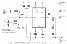
Polarity of C8 is wrong in the schematic.
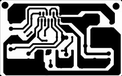
Are size and shape of C8 correct on the PCB?
How do you connect the mute/standby pin on the V+ trace with C9 on top of it?
Why are C3 and C4 of different size and shape on the PCB?
C4 should be next to the TDA's power pins.
The muting/standby circuit in the schematic is different from the PCB.
Have you tested your layout? If not, you should either mention that in the text or not publish it.
There have already been situations when newbies relied on a published design, copied it and later spent a lot of time and money only to find out that it didn't work or spent even more to tweak it and make it work.
Does the polarity of C8 matter at all, since it's connected on the NFB? It's not a trick question, I'm just curious about this.
It does not matter with regards the function, because it will see AC anyhow. It is more a convention that is left over from the times of single supply amplifiers, where the output would always be more positive than the ground. You just do it like that so that you get used to having it the right way round, should you decide to build a single supply amp one day.
The layout is very assymetrical and I expect that it will introduce hum because of the poor supply routing...
My suggestion is to go back to the drawing board and work on the routing/layout.
My suggestion is to go back to the drawing board and work on the routing/layout.
- Status
- Not open for further replies.
- Home
- Amplifiers
- Chip Amps
- PCB for TDA 7294 based amplifier - new