hi guys
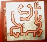
the picture uploaded below is a circuit for a buffer. after etching i did tin electroplating on it. since in our locality there is no such liquid tin.
how ever the result of the plating incomplete. the ground plane was tinned but the inner tracks were not tinned. i have tried it for so many times.
my suspection is that may be this is because of loop in the ground plane?? or something else. is this good to keep loop in ground plane.
plz help
thanks
Attachments
Last edited:
plz loot at the text also. the texts that were very closed to the ground plane got tinned. what's happening!!!
electroplating ....... with a power supply and a pair of electredes ...........
electroplating wiil make a deposit only on '' connected electrodes '' not floatiing electrodes.
electroplating wiil make a deposit only on '' connected electrodes '' not floatiing electrodes.
electroplating ....... with a power supply and a pair of electredes ...........
electroplating wiil make a deposit only on '' connected electrodes '' not floatiing electrodes.
then what is the way of doing it
Temporarily electrically connect the inner tracks to the ground plane so they can make electrical contact with the plating electrode.
electroplating ....... with a power supply and a pair of electredes ...........
electroplating wiil make a deposit only on '' connected electrodes '' not floatiing electrodes.
Didn't the old PCB procedures put the tin plate on the raw copper by using a reverse image and exposing the tracks rather than protecting them? The exposed tracks get the tin plating. The photo layer is then removed and the tin plate is the etch resist and the unprotected copper is simply etched away.
There is a similar problem with gold plated edge connectors so you have to add a section of the board with one intentional short of all the pins that gets sheared off at the end of the processing. It does make net list checking slightly tedious.
G²
Last edited:
^what about PTH?is this the same procedure by "electroplating" sir?
I don't know if the holes are drilled before or after the photoresist is applied. After the desired tracks are not protected (the photoresist is on) and the holes drilled, the plating is performed. Then the photoresist is cleaned off now exposing the areas to be etched away. The etching is done and if desired, solder mask and silk screen is applied. I haven't seen a board done this way in 20 years. The vast majority are SMOBC - Solder Mask Over Bare Copper. All the commercial boards I did from '92 to 2005 were SMOBC and most were 4 layer with an internal ground plane. The reason for SMOBC is the trace thickness is consistent so impedances are predictable vs the variable thickness plating. This may not be an issue for audio but it's important in video and computers.
G²
^Thank's sir,you give me an idea.what i think is i'll fill it with a soldering lead the hole after electroplating is performed.
- Status
- Not open for further replies.
- Home
- Amplifiers
- Solid State
- pcb electro plating