Hello,
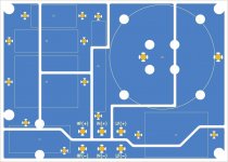
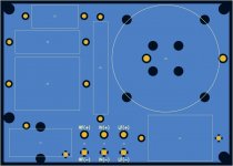
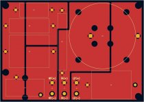
currently I'm in the progress of building a small 2 way desktop speaker, need help for the crossover PCB layout, my first attempt is make 2 layer with bottom layer as a ground plane but after browsing around seems like single layer are used for most of the passive crossover PCB then I try to make the single layer layout, is there any advantage using single layer for this purpose other than cost? I attached both of the layout and any suggestion, direction, critics are really appreciated.
Thank You
Attachments
A single layer PCB is more than enough for crossover networks, however choke placement is considered critical.
http://www.troelsgravesen.dk/coils.htm
Nescafe ? Really nice coffee.
http://www.troelsgravesen.dk/coils.htm
Nescafe ? Really nice coffee.
Hello newvirus2008, Thank You for the information, I had read http://www.troelsgravesen.dk/coils.htm article before making the layout, and yes that site is give useful information from his experiment, glad You mention here.
And about the layout, the price difference between single and double layer for 2 boards is less than $2, so is that any disadvantage if I use dual layer with ground plane in the bottom layer?
PS: my favorite Nescafe ☕ is the old "analog" plain one 🙂
And about the layout, the price difference between single and double layer for 2 boards is less than $2, so is that any disadvantage if I use dual layer with ground plane in the bottom layer?
PS: my favorite Nescafe ☕ is the old "analog" plain one 🙂
There may not be any disadvantage as such, but then if I were you I would use that extra money to get double copper thickness on the top layer instead.
Yes, both Nescafe still available, somehow I seem to like it with the chicory though. 👍
Yes, both Nescafe still available, somehow I seem to like it with the chicory though. 👍
Unfortunately the available thickness is only 1oz, but that is a good idea, how if I make same pour for top and bottom and then stich using via, is that better than previous idea using ground plane on bottom?
Thank You.
Thank You.
"Ground plane" as low inductance shielding surface is completely irrelevant for a passive high current audio frequency crossover. Many people prefer point-to-point soldering and mounting on small wooden board for this application, however you may find a pcb useful for mechanical mounting of parts.
Just make traces wide for high currents, consider additional holes for strapping inductors and keep inductors separated from eachother. And keep in mind inductors are heavy and loudspeakers vibrate, so firm (and non-rattling) mounting of pcb to the box is important!
Just make traces wide for high currents, consider additional holes for strapping inductors and keep inductors separated from eachother. And keep in mind inductors are heavy and loudspeakers vibrate, so firm (and non-rattling) mounting of pcb to the box is important!
Last edited:
If you have concerns over the current carrying capacity of the 1 oz. you can always loose the solder mask and "tin" the traces with a layer of solder. Not the prettiest solution but it works.Unfortunately the available thickness is only 1oz,
Yes, that is definitely a good idea. Also, you may not need the stitching part, as the plated through-holes would do that for you, for free. Just make sure that every node has a hole, which should be fairly straightforward, as crossover parts are seldom SMD.how if I make same pour for top and bottom and then stich using via, is that better than previous idea using ground plane on bottom?
I consider the ground plane irrelevant because all the points in a crossover network are at low-impedance and are therefore unlikely to pickup any noise / stray signals. The plane, however, is primarily meant to reduce noise pickup by providing coupled return paths for the respective currents.
If you plan to solder-coat the tracks as mentioned by techtool, you may also ask for omission of the solder mask altogether, which might reduce the price a little. You could also spray a thin clear coat (of whatever) after assembly, if meant for use in a corrosive environment (ship etc.).
Another fabrication-related option would be to opt for double thickness (3.2mm) of PCB, considering the vibrations the network would be subjected to, especially if being placed inside the speaker enclosure. This would also solve Stv's concerns regarding the heavy inductors.
Last edited:
@stv: that is actually the main question, so that is irrelevant, Thank You for the direction.
@techtool, will consider the idea, Thank You
@newvirus2008, noted, the idea of using via is to help make the impedance lower
OK Thank You everybody for enlighten me, Have A Nice Weekend and Happy Easter 🙂
@techtool, will consider the idea, Thank You
@newvirus2008, noted, the idea of using via is to help make the impedance lower
OK Thank You everybody for enlighten me, Have A Nice Weekend and Happy Easter 🙂

- Home
- Loudspeakers
- Multi-Way
- Passive Crossover PCB Layout Question