Channels 1 and 2 are operating correctly, and only channel 3 is misbehaving, right?
Opamp U3 has the proper +/- 12V on its supply pins, right?
Assuming the above is the case, would you perform the following test:
Set input level R79 to max, but leave input jack open. (I want max bias resistance available to Q30.) Apply power and get the amp into the state you described earlier, i.e. about -1.46V at channel 3 output. Then please report the following voltages re ground:
Gate of Q30 (amp input)
Gate of Q29 (amp feedback)
Junction of R65, C130, R218. (This node should be effectively the amp output, but before the relay.)
U3 pin 6 (servo out)
I hope data this will point us in the right direction.
Thanks!
Channels 1 and 2 are operating correctly, and only channel 3 is misbehaving, right? CORRECT.
Opamp U3 has the proper +/- 12V on its supply pins, right? NO. WITH AMP POWERED, I SEE HUGE DIFFERENCE ON +Vs Pin 7 BETWEEN CHANNELS 1/2 & CHANNEL 3. CHANNELS 1/2 READ 14.4 VDC, CHANNEL 3 READS 0.7 VDC.
Assuming the above is the case, would you perform the following test:
Set input level R79 to max, but leave input jack open. (I want max bias resistance available to Q30.) Apply power and get the amp into the state you described earlier, i.e. about -1.46V at channel 3 output. Then please report the following voltages re ground:
FYI, STEADY-STATE DC OFFSET WITH R79 @ MAX IS (previously stated) 1.4 Vdc, STEADY-STATE DC OFFSET WITH R79 @ MIN IS 1.0 Vdc.
Gate of Q30 (amp input) HAVE NOT PERFORMED THIS TEST YET. GATE IS MIDDLE PIN OF THAT JFET AND DIFFICULT TO ACCESS SAFELY.
Gate of Q29 (amp feedback) SAME AS ABOVE.
Junction of R65, C130, R218. (This node should be effectively the amp output, but before the relay.) READS ESSENTIALLY SAME AS THE VALUE AT THE SPEAKER OUTPUT.
U3 pin 6 (servo out) YES, AGAIN READS ESSENTIALLY SAME AS THE VALUE AT THE SPEAKER OUTPUT.
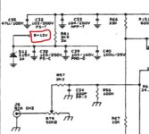
SO, LIKELY ROOT CAUSE IN IN B+ REGULATION FOR CHANNEL 3 ?? SEE SCHEMATIC PIC. NOTE; I ALREADY REPLACED C40. ALSO, R81 IS EXACTLY TO SPEC. I MAY REMOVE THE BOARD AND OHM OUT EVERYTHING THERE (AGAIN) BEING SURE TO CHECK FOR CONTINUITY AT EACH AND EVERY SOLDER JOINT.
THOUGHTS?
Opamp U3 has the proper +/- 12V on its supply pins, right? NO. WITH AMP POWERED, I SEE HUGE DIFFERENCE ON +Vs Pin 7 BETWEEN CHANNELS 1/2 & CHANNEL 3. CHANNELS 1/2 READ 14.4 VDC, CHANNEL 3 READS 0.7 VDC.
Assuming the above is the case, would you perform the following test:
Set input level R79 to max, but leave input jack open. (I want max bias resistance available to Q30.) Apply power and get the amp into the state you described earlier, i.e. about -1.46V at channel 3 output. Then please report the following voltages re ground:
FYI, STEADY-STATE DC OFFSET WITH R79 @ MAX IS (previously stated) 1.4 Vdc, STEADY-STATE DC OFFSET WITH R79 @ MIN IS 1.0 Vdc.
Gate of Q30 (amp input) HAVE NOT PERFORMED THIS TEST YET. GATE IS MIDDLE PIN OF THAT JFET AND DIFFICULT TO ACCESS SAFELY.
Gate of Q29 (amp feedback) SAME AS ABOVE.
Junction of R65, C130, R218. (This node should be effectively the amp output, but before the relay.) READS ESSENTIALLY SAME AS THE VALUE AT THE SPEAKER OUTPUT.
U3 pin 6 (servo out) YES, AGAIN READS ESSENTIALLY SAME AS THE VALUE AT THE SPEAKER OUTPUT.
SO, LIKELY ROOT CAUSE IN IN B+ REGULATION FOR CHANNEL 3 ?? SEE SCHEMATIC PIC. NOTE; I ALREADY REPLACED C40. ALSO, R81 IS EXACTLY TO SPEC. I MAY REMOVE THE BOARD AND OHM OUT EVERYTHING THERE (AGAIN) BEING SURE TO CHECK FOR CONTINUITY AT EACH AND EVERY SOLDER JOINT.
THOUGHTS?
Attachments
Yes, first you have to repair whatever ails the B+ to U3. Know how to troubleshoot that? If you happen to have installed an IC socket, remove the IC for reduced confusion. If soldered, leave in place.
I often tack some hookup wire to points of interest so I can safely bring them to the outside for probing. Anchor them with tape to prevent accidents.
I often tack some hookup wire to points of interest so I can safely bring them to the outside for probing. Anchor them with tape to prevent accidents.
More musings:
Check D11 orientation. If backward, you'd see about 0.7VDC
R81 should be toasty warm if working. Should be ~~50V across R81 leads.
If you discover D11 or R81 is defective, you could remove them and jumper U3's B+ to another channe's B+. There should be enough bias current to supply two channels while you get replacements and this would allow you to pursue further troubleshooting.
You can also lift one end of R70 and explore amp bias without servo correction--- the amp should bias without it. The fact that output shifts with rotation of level pot is also suspicious.
I think we're making progress.
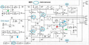
Long story short. I have swapped various components (see attached) and the Channel 3 symptoms, large fluctuating DC offset and subsequent protection circuit tripping, have been resolved. But I'm writing for some advice because there's still something not quite right.Forgot to mention you should also monitor the +/-12V servo supply to see how that compares between the 2 channels.
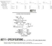
Way back bullittstang suggested that I "...move to the JFETs, Q26, Q28, Q29, Q30". After other ill fated parts swaps, when I finally acquired new Toshiba JFETs the problem was resolved. Yet I now see a steady Ch3 offset of 0.016 V where as Ch1 and Ch2 offsets are both ZERO. I can live with that, but recall this amp has a servo. Furthermore, I did long ago, upon comments from BSST, replace the AD711 servo. As servo function depends upon +Vs and -VS (see attached), I checked B- vs B+ and for each of the three channels it reads: Ch1 B-/B+: 28.92 V, Ch2 B-/B+: 29.24 V, Ch3 B-/B+: 30.13 V. Can such variation in supply voltage cause a steady state error out of the servo for Ch3?
I can reinstall the original AD711 op-amp if there's reason to believe such chips exhibit such variation. Or perhaps I should attempt to diagnose the variation in B- B+.
BTW, R82 and R83 were overheated after I replaced BJT's Q25/Q27/Q31/Q34 with, what turned out to be crappy eBay parts. I reinstalled the both original 2SC2240 and 2SA970 pairs. Caps C35 and C123 were long ago replaced.
Any thoughts on next steps would be appreciated.
Attachments
By my reading of schematic, supply pins on the servo opamp should be +12V, -12V. Are you saying each pin is about 30V, or about 30V rail to rail?
What is PA amp output DCV?
What is PA amp output DCV?
Ch1 B-/B+: 28.92 V, Ch2 B-/B+: 29.24 V, Ch3 B-/B+: 30.13 V. Can such variation in supply voltage cause a steady state error out of the servo for Ch3?
The AD711 specs (see abbreviated specs attached) states Vs = +/- 15 Volts. I suspect the Parasound schematic is incorrect. (Errors in there documentation seems not uncommon.)
My readings are rail to rail.
I don't have the knowledge to answer "What is PA amp output DCV?". I spent the last 30 minutes reading on the subject but, as more a mechanical controls engineer (retired), am probably more confused after reading on the topic.
I've read much of the AD711 spec sheet and can't see any stated open-loop error limit specified, nor do I see anything to about Vs to raise an eyeborow (except, perhaps, a foot note about "exceeding –14.1 V negative common-mode voltage on either input results in an output phase reversal".
BTW, I have two new observations to report.
1) I turned it on and saw DC offset settle to a slightly higher value (0.020 Vdc, was 0.016 V), and the rail to rail voltage for that channel now also slightly higher (30.4 V, was earlier 30.13 V).
2) There's definitely more heat in the heat sink for Channel 3 than the others (Note: there are two heat sinks and three channels with, effectively one and a half output stages occupying each sink). I checked bias and saw it was rather high (42 mV). I've adjusted all three channel's bias to 15 mV. I've check sink temps with Fluke thermometer and am satisfied with temp and balance. After 40 minutes of idling the Ch3 offset is stable at 0.015 V while rail to rail is still 30.4 V.
Attachments
Another observation. A bit of freeze spray on the servo will cause an instantaneous reduction in the DC offset, though it doesn't simply go to zero.
The opamp supply voltages are probably OK, but if you can locate/determine a Zener type number you may be able to confirm the design was revised to +/-15V.
"PA output" was intended as Power Amp output, aka speaker voltage, etc. You're measuring what I was seeking. 😀
The output voltages you observe are not bad. But that said, they are a bit higher than expected given the low offset error spec'd for the AD711. What voltage do you observe at pin 6 of the AD711? It should be a few volts at most, not near either opamp rail. If voltage as is described, measure the voltage between opamp pins 2 and 3; this is the opamp offset error and is specified as less than 0.25mV. Ideally, this is the error you'd also find at the speaker terminals. If you wish to pursue the discrepancy, look at voltage drops from pin 2, through R69 to speaker minus terminal. In similar manner, explore drops from pin 3, through R210 to speaker plus terminal. Symptoms suggest there are unintended DC drops across these paths. They are probably of no concern, but interesting to understand.
Are you able to post the pdf of your schematic? It seems to be different than what I found on the web.
Thanks.
Have you checked the DC going into the OpAmp? I’m guessing it is high and it can’t quite make up the difference? But if it’s 15-20mV on the speaker, I would call it good unless you want to match and change the input BJT pairs (C2240/a970) bc those input Fets are expensive since they obsolete and have to buy ones from the DIYAudio store but it’s all your choice. I’m guessing if there’s high DC going into the OpAmp that one or two of those BJT are breaking down internally and no longer matched well enough.
Hi bullittstang,
The DC servo should automatically correct this issue unless the input differential pair is terribly mismatched or failed. If this is the case, the DC servo opamp output will be pinned to one of its supply rails. That will tell the story, I believe.
The DC servo should automatically correct this issue unless the input differential pair is terribly mismatched or failed. If this is the case, the DC servo opamp output will be pinned to one of its supply rails. That will tell the story, I believe.
Pin 6 = 0.114 V.
Measuring voltage between pins 2 and 3 is a bit unnerving due to packaging constraints. My probes don't really get in there (safely). I'll need time to devise a couple of separated wire leads to get at it. Yes, I'd like to get that reading and see if it exhibits a discrepancy to the output I'm seeing at the speaker terminals (i.e., I get your logic). If something;s there, yes again, perhaps I can trace down what could be unintended DC drops. (Probably deeper diagnosis than I've ever taken on, but doable.)
I've posted all that I've ever had in the way of a HCA-2003 schematic pdf. (They made a handful of HCA-2003a which included a DC trigger feature.) The input board "B2030" is on the left side in the schematic, channels 1 at left top, 3 at left bottom. Power supplies board "B2032" on far upper right.
Thanks. Progress, it seems.
Attachments

Yep, those JFETS were $36 for the two pair (Toshiba 2SJ74 + 2SK170 LAB MATCH QUAD to 0.1mA (7.0 - 9.0 mA range "BL" "B")).
I can "live" with 0.014 V offset (having lived with and repaired old Hafler amps which go adrift every decade or so...) so long as it remains stable. But, of course, even so it's simply not functioning correctly.
I want to be able to relax when using it to drive some expensive transducers.
I want to be able to relax when using it to drive some expensive transducers.
- Home
- Amplifiers
- Solid State
- Parasound Amp Unstable Channel Output - Seeking Troubleshooting Advice