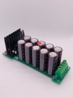
I built an amplifier using several TDA7293 chips connected in parallel to make good use of my extra stock. The result honestly surprised even me!
I added a buffer stage at the input using opamps like the OPA1641, OPA1655, or OPA627, because I'm using an ALPS RK27 potentiometer for volume control directly at the output of a NOS DAC.
If you prefer, you can easily disable the buffer. Simply remove the opamp and short pins 2 and 3 of the socket.
In this case, R2 should be 47K, and you should remove both C23 and R1.
If you would like to keep an RC-filtered input instead, use R1 = 100Ω and C23 = 100pF.
Now, I’m excited to share some measurements with you!
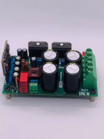
EPIC W

1W Measurement (2x42VDC)

Output Noise (input shorted)

Schematic

Positive Regulator

Negative Regulator

I added a buffer stage at the input using opamps like the OPA1641, OPA1655, or OPA627, because I'm using an ALPS RK27 potentiometer for volume control directly at the output of a NOS DAC.
If you prefer, you can easily disable the buffer. Simply remove the opamp and short pins 2 and 3 of the socket.
In this case, R2 should be 47K, and you should remove both C23 and R1.
If you would like to keep an RC-filtered input instead, use R1 = 100Ω and C23 = 100pF.
Now, I’m excited to share some measurements with you!
EPIC W
1W Measurement (2x42VDC)
Output Noise (input shorted)
Schematic
Positive Regulator
Negative Regulator
Attachments
Last edited:

Though chip amplifiers often earn the scorn of audio purists, I must contend that, when measured against countless LM3886 implementations and other such designs, this particular amplifier stands out as one of the finest chip amps I have ever encountered. Boasting a remarkably low 0.00054% THD and an impressive 103 dB SNR in its dual-parallel TDA7293 configuration, it has nonetheless been deprived of the recognition it so richly deserves. I trust this observation will prove helpful to fellow forum members.
When looking at the THD plot:
2nd harmonic -98dB which translates into 0.00126%
3rd harmonic -110dB which translates into 0.00032%
4th harmonic -104dB which translates into 0.00063%
and so on for the rest.
Just these 3 harmonics contribute for ~0.002% THD.
Where that 0.00054% comes from? It doesn't add up with the math. Something is not right.
The datasheet's numbers are quite different as well.
I like TDA7293 however the longer term future is TPA3255.
Gain at 10 should deliver 0.001% at 8 ohms with no op amp help.
Gain at 10 should deliver 0.001% at 8 ohms with no op amp help.
Are you suggesting my measurements are fake? When I tested the TDA7293 with the exact same components as the datasheet circuit, I obtained identical results with datasheet. With a well-designed PCB, high-quality components, and the TDA7293 set to 10× gain, the performance improvements are substantial. These measurements are genuine. If you’d like to verify for yourself, I can send you a PCB! Additionally, you should sum these harmonic components logarithmically—in dB—rather than linearly.When looking at the THD plot:
2nd harmonic -98dB which translates into 0.00126%
3rd harmonic -110dB which translates into 0.00032%
4th harmonic -104dB which translates into 0.00063%
and so on for the rest.
Just these 3 harmonics contribute for ~0.002% THD.
Where that 0.00054% comes from? It doesn't add up with the math. Something is not right.
The datasheet's numbers are quite different as well.
Note: A unity-gain op-amp stage has no effect on SNR or THD. The measurements were also performed with the op-amp bypassed.
Gonkar:
You should read carefully the incriminated plot.
The signal level is NOT 0dBV, as you hastily suppose in your calculations.
As indicated, it is 1W/8ohm, 2,841Vrms: that is +9dBV level.
2nd harm is ~-107dBV,
3d harm is ~-119dBV,
4th harm is ~-113dBV
A quick back of the hand approximation: the reported result 0,00054% had been referred to 2,841Vrms level.
Your calculations are referring to 2,841 times lower level, 1Vrms.
So your calculation should report 2,841 times worse result. That is, 0,00054%*2,841= 0,00153%.
I think it is close enough to show the root cause of your misunderstanding.
Have a nice day, George
Last edited:
I am a huge fan of using two TDA7293 for higher power.
However, what you call Parallel can be misleading.
That term is best used in the LM3886 when two chip amps are used to drive the load.
In the TDA7293, the way it's configured is totally different.
The Master amp is the main amp.
The second TDA7293 is the Slave.
In the Slave, the voltage section is not used. Only the power mosfets.
It's no different from a discrete design when you add more power transistors for higher power
The circuit in Fig 11 shows clearly the way the two TDA7293 are used.
The Buffer Driver in the Master drives the mosfets of the Slave.
In fact, an internal switch even disconnects the Slave's voltage stage in the Slave.
ST calls this Modular configuration.

Regarding THD, Figure 15 is the Distortion vs Output Power measurements.
At 1W/1KHz, THD is at 0.007%.
Frankly, more zeros to me are meaningless.
sercan85 should be commended for highlighting this method of using two TDA7293 for higher power.
Regards
Mike
AmpsLab

However, what you call Parallel can be misleading.
That term is best used in the LM3886 when two chip amps are used to drive the load.
In the TDA7293, the way it's configured is totally different.
The Master amp is the main amp.
The second TDA7293 is the Slave.
In the Slave, the voltage section is not used. Only the power mosfets.
It's no different from a discrete design when you add more power transistors for higher power
The circuit in Fig 11 shows clearly the way the two TDA7293 are used.
The Buffer Driver in the Master drives the mosfets of the Slave.
In fact, an internal switch even disconnects the Slave's voltage stage in the Slave.
ST calls this Modular configuration.
Regarding THD, Figure 15 is the Distortion vs Output Power measurements.
At 1W/1KHz, THD is at 0.007%.
Frankly, more zeros to me are meaningless.
sercan85 should be commended for highlighting this method of using two TDA7293 for higher power.
Regards
Mike
AmpsLab
I’m fully aware that this isn’t a parallel connection—it’s just a figure of speech, out of habit. This amp sounds so good that even my wife said “wowww, how did you make this?” the first time she heard it. The best part is that the OPA1641 and OPA1655 op-amps, used in unity gain, have an audible impact on the sound but absolutely no measurable effect—whether good or bad. For someone like me who listens to music with a NOS DAC and uses a potentiometer, this amp does an excellent job. I can wholeheartedly recommend it—an amazing amplifier.
I'm with you on this.
I feel the TDA7293 is vastly under-rated in the DIY community.
In the commercial world, it's very popular.
Bose for one, uses the TDA7293 in their Lifestyle SA series amplifiers.
They chose to run it in Class H for whatever reason.
The only gripe I have with the TDA chip amps, the 7293 included, is they are hum prone.
It always take me a few pcb layouts to get it hum free.
The hum is not loud but audible at 3ft.
I never get hum in my discrete designs.
Never with STK amps and LM3886.
Only with TDA.
Maybe it's just me.
Below is my TDA7293 Modular amp.
It took five revisions, hence V5, to get it hum free.
I get 125W into 4 ohms and 70W into 8 ohms clean power just before clip.
That's incredible for a chip amp.
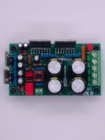
So far, none of the amplifiers I’ve built have ever suffered from hum or ground-loop issues. The only time I’ve observed high output noise was due to poor circuit design or the use of inappropriate components. In TDA7293-based projects—and in amplifier PCB layouts in general—the single biggest mistake is routing the signal-reference grounds and the power ground on the same plane, thereby creating a loop. No matter how you arrange your ground traces, be sure to avoid any ground-plane loops.
You’ll see this principle illustrated beautifully in the PCB examples of leading brands like Sony, Marantz, Denon, and Sansui in their service manuals. In fact, with the input shorted, this amp exhibits just 18 µV of noise—practically inaudible. I may well be the first person to run the TDA7293 at a gain of 10×, and the results are outstanding. I highly recommend you try it yourself.
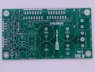
If you’d like to experiment, I’d be happy to send you a pair of EPIC W PCBs—four-layer, professional-grade boards. Let me know!
You’ll see this principle illustrated beautifully in the PCB examples of leading brands like Sony, Marantz, Denon, and Sansui in their service manuals. In fact, with the input shorted, this amp exhibits just 18 µV of noise—practically inaudible. I may well be the first person to run the TDA7293 at a gain of 10×, and the results are outstanding. I highly recommend you try it yourself.
If you’d like to experiment, I’d be happy to send you a pair of EPIC W PCBs—four-layer, professional-grade boards. Let me know!
Attachments
Thanks for the offer but I'm good for now.
Don't have much time for electronics.
Once I get my gardening done, I need to restart designing speakers.
Just out of curiosity, why do you need a 4-layer board?
I use 2-layers. The top is the ground plane for power/dirty ground.
The signal ground is at the bottom.
Don't have much time for electronics.
Once I get my gardening done, I need to restart designing speakers.
Just out of curiosity, why do you need a 4-layer board?
I use 2-layers. The top is the ground plane for power/dirty ground.
The signal ground is at the bottom.
A common mistake many people make in PCB design is making the power supply traces and output traces too thin. For this 150W amplifier, the power supply and output traces need to be thick. Additionally, minimizing PCB size, avoiding vias on the signal path, and similar considerations are very important. The fact that JLCPCB offers very affordable prices for 4-layer boards is a great advantage.
Looks very good Sercan. I have been bonded to the LM series of chip amps for the last few years, it must be time to try the 7293.
Your parrallel design looks like a good candidate.
What voltage are you running the rails at ? Do you think there is an optimum value for best performance ?
In your circuit what are the values of R6 and R7 ?
Nice compact design on the board.
Your parrallel design looks like a good candidate.
What voltage are you running the rails at ? Do you think there is an optimum value for best performance ?
In your circuit what are the values of R6 and R7 ?
Nice compact design on the board.
Thanks
R6:47k nfb resistor(cmf60 0.1%)
R7:10ohm zn resistor
Voltages: 2x42vdc (2x30vac transformer)
I’ve done so many tests with the TDA7293 that I’ve found the optimal NFB resistor values for 10x gain to be 47k/4.7k. This configuration delivers the best results in terms of both noise and THD. Interestingly, with the LM3886, the ratio of the NFB resistor doesn’t have such a significant impact.
If your PCB layout is well-designed, it’s practically impossible to make the TDA7293 oscillate. That’s why I chose 10 ohms for R7, one of the most commonly used values. This results in a higher cutoff frequency. While the datasheet recommends a 3.9-ohm resistor with a 1uF capacitor for the Zobel network (resulting in a cutoff around 40kHz), I decided not to include it since I observed no signs of oscillation during testing.
What truly sets the TDA7293 apart from other chip amplifiers is its modular nature.
So far, I’ve developed two projects based on the TDA7293: one is a JFET-buffered CFB amplifier, and the other is this current design. I have several more unique ideas in mind; if I manage to implement them successfully, they could lead to some very interesting results.
Finally, if you’re building a TDA7293 amplifier for the first time, I highly recommend starting with a simple, well-proven design like a parallel or "epic W" topology.
- Home
- Amplifiers
- Chip Amps
- Parallel TDA7293 with Input Buffer