Greets & thanks to the community, been through a lot of threads that have proven quite helpful.
Hoping I could get input on whether this board layout is functional/optimal, first timer here.
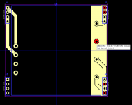
Power comes in via a DC-DC converter on J4 that's mounted to a seperate board.
My biggest concerns are whether the set pin layout is ok, the datasheet suggests a guard ring & I'm not fully sure I've accomplished that here. That and there aren't any great examples of a parallel 3094 layout, so just horked ideas from the 4x 3045 design on AD's website.
I might have to break the whole thing out into a seperate sub-assembly so that I can follow the exact layout of the eval boards? This area is all the space that's available on the mainboard. Are there any designs floating around the forum that would be good examples of a parallel 3094 layout?
Cheers & much appreciate all help and suggestions
Hoping I could get input on whether this board layout is functional/optimal, first timer here.
Power comes in via a DC-DC converter on J4 that's mounted to a seperate board.
My biggest concerns are whether the set pin layout is ok, the datasheet suggests a guard ring & I'm not fully sure I've accomplished that here. That and there aren't any great examples of a parallel 3094 layout, so just horked ideas from the 4x 3045 design on AD's website.
I might have to break the whole thing out into a seperate sub-assembly so that I can follow the exact layout of the eval boards? This area is all the space that's available on the mainboard. Are there any designs floating around the forum that would be good examples of a parallel 3094 layout?
Cheers & much appreciate all help and suggestions
Attachments

LTSpice shows the -12V out that I'm after, but my boards are a different story - just -0.12V OUT/OUTS, and the floating VIOC pin shows -1.38V.
Anybody familiar with these that can see something I'm not seeing?

Anybody familiar with these that can see something I'm not seeing?
I would check the soldering first. I've seen strange behaviour with LT3094 when one or more pins were not properley soldered.
Are the 2 GND pins on J4 connected at the other board?
Are the 2 GND pins on J4 connected at the other board?
That's a good call. We've had the same result with 3 seperate boards, I installed the LT3094's with stencil & flow wand.I would check the soldering first. I've seen strange behaviour with LT3094 when one or more pins were not properley soldered.
Are the 2 GND pins on J4 connected at the other board?
Thanks. Yes the 2 ground pins are normalized on the other board to the COM (ground) of the DKA30A-12 as shown in this pic.
Attachments
Have you tried a bench power supply for the regulators alone (i.e. without DC-DC converter)? That would also give you the current at idle which should be less than 10mA.
I did, thanks!Have you tried a bench power supply for the regulators alone (i.e. without DC-DC converter)? That would also give you the current at idle which should be less than 10mA.
Turns out I had the wrong Set resistor installed - somehow got a 60.4Ohm instead of 60.4K, so that'll take care of it.
Really appreciate your help
- Home
- Amplifiers
- Power Supplies
- Parallel 3094 Design