Hi Guys,
I have DSE a2760 amp which I am trying to make it a dedicated power amp. However the right channel has developed some issue of burning output transistor 2SC5200, which had 0 ohms between base and emitter.
I measured the voltage across the output resistors between the two push-pull out transistors and the voltage is climbing up to 60mv, while the left channel remains 34mv, which is good.
I have bought another 2sc5200, and installed it there. I keep an eye on the voltage, which rised upto interestingly 40mv, and now remains 0.
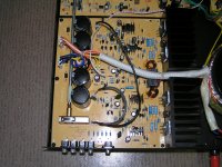
Can anyone help me to solve this problem? Thanks in advance. The schematic is attached here.

I have DSE a2760 amp which I am trying to make it a dedicated power amp. However the right channel has developed some issue of burning output transistor 2SC5200, which had 0 ohms between base and emitter.
I measured the voltage across the output resistors between the two push-pull out transistors and the voltage is climbing up to 60mv, while the left channel remains 34mv, which is good.
I have bought another 2sc5200, and installed it there. I keep an eye on the voltage, which rised upto interestingly 40mv, and now remains 0.
Can anyone help me to solve this problem? Thanks in advance. The schematic is attached here.
You need to check the previous transistor D669 on the schematic as well, as a faulty transistor there could also give you those symptoms .
Last edited:
You need to check the previous transistor D669 on the schematic as well, as a faulty transistor there could also give you those symptoms .
thanks I did that. It appears that they are good. (by simple resistance measure.)
Check your bias current by measuring voltage across the .39ohm emitter resistors. Compare with good channel. You need to monitor bias as temperature changes. If it is high compared to the good channel, look for problems in bias circuit and/or constant current source transistor feeding bias circuit.
Let me know your idle current, and how it compares to good channel as temperature changes. You said it remains zero. Is it zero all the time now?
Let me know your idle current, and how it compares to good channel as temperature changes. You said it remains zero. Is it zero all the time now?
Last edited:
Check your bias current by measuring voltage across the .39ohm emitter resistors. Compare with good channel. You need to monitor bias as temperature changes. If it is high compared to the good channel, look for problems in bias circuit and/or constant current source transistor feeding bias circuit.
Let me know your idle current, and how it compares to good channel as temperature changes. You said it remains zero. Is it zero all the time now?
the voltage across emitter resistors are 17.4mv and 17.4mv with good channel.
bad channels are now all 0, which means the bias is gone?
It also devoleped changing DC output to speakers on the bad channel, though there is sound from the speaker. (it still does the job!)
I couldn't find anything wrong with the circuit and that is why I am asking for help.
Thanks,
Last edited:
V205 is a clamp to establish bias. It sets bias voltage. If it is shorted Collector to Emitter, idle current would be zero. The voltage of clamping is set by resistors r207 r208 and r209 in a divider for the base. The current from the current source is also relevant here (V213).
V205 is a clamp to establish bias. It sets bias voltage. If it is shorted Collector to Emitter, idle current would be zero. The voltage of clamping is set by resistors r207 r208 and r209 in a divider for the base. The current from the current source is also relevant here (V213).
thanks, it is not shorted.
Usually, the BJT failure mode is a C-E short but when there is a B-E short, the current from the driver will be maintained, almost always blowing it too. These aren't the toughest drivers around so I have my doubts about their survival. The most likely cause would be a shorted output in the connectors, leads, speaker, crossover etc. but there is VI limiting protection which should have clamped output stage current at a safe limit and you would have noticed the increased heating. Possibly, the limiter circuitry is now toast too.
Resistance measurements aren't telling you enough. You need to measure that the Vbe of those drivers is around 0.65V before declaring them OK, whether the output transistors are dead or not but check that R288 or R271 are OK to allow this. Remove and test the drivers properly if you can't do that with the amp. powered as is. Also, don't leave speakers or any input signal connected when DC testing a power amp.
Resistance measurements aren't telling you enough. You need to measure that the Vbe of those drivers is around 0.65V before declaring them OK, whether the output transistors are dead or not but check that R288 or R271 are OK to allow this. Remove and test the drivers properly if you can't do that with the amp. powered as is. Also, don't leave speakers or any input signal connected when DC testing a power amp.
Usually, the BJT failure mode is a C-E short but when there is a B-E short, the current from the driver will be maintained, almost always blowing it too. These aren't the toughest drivers around so I have my doubts about their survival. The most likely cause would be a shorted output in the connectors, leads, speaker, crossover etc. but there is VI limiting protection which should have clamped output stage current at a safe limit and you would have noticed the increased heating. Possibly, the limiter circuitry is now toast too.
Resistance measurements aren't telling you enough. You need to measure that the Vbe of those drivers is around 0.65V before declaring them OK, whether the output transistors are dead or not but check that R288 or R271 are OK to allow this. Remove and test the drivers properly if you can't do that with the amp. powered as is. Also, don't leave speakers or any input signal connected when DC testing a power amp.
Thanks for your reply.
Now the amp is running with voltage across R271(faulty channel) being 10mv higher than R212(OK channel). The target should be both around 34mv for right bias.
Drivers Vbe are all around 0.6v, so I assume all transistors are OK.
So it is running slightly hotter.
Measure voltage across R228. (compare to same resistor in good channel.) The voltage should be one junction (about .7 volts). This current source has to work properly for the bias circuit to work. Let me know the result. Do you have an oscilloscope?
Measure voltage across R228. (compare to same resistor in good channel.) The voltage should be one junction (about .7 volts). This current source has to work properly for the bias circuit to work. Let me know the result. Do you have an oscilloscope?
It is 0.616 for R228(left channel), and 0.612 for R277(right channel, bad one).
Unfortunately I don't have an oscilloscope. Perhaps I should build one using my computer.
Thanks for your reply.
Now the amp is running with voltage across R271(faulty channel) being 10mv higher than R212(OK channel). The target should be both around 34mv for right bias.
The voltage across R271 should be higher (2 junctions). Did you mean emitter resistor R211 or equivalent for the 32mv?
Emitter resistor voltage is just half that of r271/r212.The voltage across R271 should be higher (2 junctions). Did you mean emitter resistor R211 or equivalent for the 32mv?
Interestingly, now these numbers are all zero after running a while.
The heat sink on fsulty channel is cool.
R262 or R212 should be twice that of the emitter resistors. Those are across npn and pnp output emitter resistors.
Are you saying both channels have zero voltage across these resistors? (R262 and R212)
Are you saying both channels have zero voltage across these resistors? (R262 and R212)
R262 or R212 should be twice that of the emitter resistors. Those are across npn and pnp output emitter resistors.
Are you saying both channels have zero voltage across these resistors? (R262 and R212)
Only the faulty channel.
Interestingly, it climb up to around 42mv, which is too high, and after 20 minutes it will down to 0.
The bias transistor is supposed to compensate for heat. It is overcompensating to cutoff. On the good channel how much does the bias change after warm up?
What is the collector to emitter voltage on V205 when bias drops to zero? What is it on the good channel after warmup?
What is the collector to emitter voltage on V205 when bias drops to zero? What is it on the good channel after warmup?
Last edited:
The bias transistor is supposed to compensate for heat. It is overcompensating to cutoff. On the good channel how much does the bias change after warm up?
What is the collector to emitter voltage on V205 when bias drops to zero? What is it on the good channel after warmup?
I have swapped v205 and v206, now the bias voltages are stable at 25.5mv and 29.9mv respectively. slightly different than before, which is 19mv and 40mv.
It might be the problem of soldering but I am not sure.
However the right channel DC output on speakers is still not stable, changing between 40mv and -40mv, which is quite unsettling.
Maybe the components are not stable?
They are on the main heat sink.It seems V205, V206 are TO92 transistors. How are they connected to the heatsink?
I think there are different revisions of the design and PCB. These were well constructed Korean products and used good components but were problematic. When sold about 15-20 years ago, there were many return claims and the repaired units were sold off cheaply, which is when cheapskates like me paid not much more than AU$100.
V205 and V206 are actually TO220 transistors, attached to the 'sink in my example too.
http://www.overclockers.com.au/wiki/images/c/c3/A2760_Preamp_Bypass.jpg
V205 and V206 are actually TO220 transistors, attached to the 'sink in my example too.
http://www.overclockers.com.au/wiki/images/c/c3/A2760_Preamp_Bypass.jpg
Attachments
- Status
- Not open for further replies.
- Home
- Amplifiers
- Solid State
- output transistor keeps burning, need help.