Have you tested the diode? It seems that the amplifier is doing proper by heating up slowly until a point, but the specification says 18 mV, so it's heating up a bit too much.
1st: does the amplifier work otherwise?
2nd: both channels are the same, which is a good thing.
3rd: Check the trimmer pots - are they truly at 0 ohms when turned all the way down? Does bias increase if you turn the trimmer the other way?
1st: does the amplifier work otherwise?
2nd: both channels are the same, which is a good thing.
3rd: Check the trimmer pots - are they truly at 0 ohms when turned all the way down? Does bias increase if you turn the trimmer the other way?
Thanks Mooly about the small transistors as i was tempted to replace them but no need to now.
Hi Orbanp
R1 and R3 are good. I tested the diode with a 1k resistor and the forward stv 04 at 4mA it read 2.13v just in case my meter was playing up I also did 4x1n4148 in series using the same set up they read 2.64v
Hi Mrcloc
the amp works perfectly with no known distortion,
Yes both channels are the same in readings this amp as dual power supply so there is even no common ground there,
The trim pots are right down but if turned them up the bias goes up also. Is it possible the trim pots can become unstable?
Hi East Electronics
the only parts that i have replaced is the driver transistors on one channel (which made not a pip squeek of difference) all the power amp boards look also most un touched apart from a power transistor may have been replaced as there is evidence scratch marks around a solder joint
Do the output transistors have the same type number as shown in the manual ?
I mentioned at the start that this bias arrangement was 'fussy' and while the transistors fitted will not be faulty, you could well find that modern replacements behave differently.
For information...
A well designed bias circuit should maintain the set bias from a cold start right the way through the normal operating temperature range of the amplifier. I think we were less concerned with that kind of stability many years ago but the bias should certainly stay within say 30 to 40% of its set value and also reach that value after only a couple of minutes of being powered up.
I looked at some other older Kenwood amps of similar age and they to seem to have the bias set way below the optimum value (for reasons of reliability and cool running).
Simplest option is just to 'fiddle' the circuit by adding a single resistor across the diode pack.
Best option would be to replace the diode with a properly designed conventional Vbe multiplier.
I will try the resistor across the diode.
It does seem unusual why the amp has to be modified to bring it to do something it should be doing its self,
Is it worth taking the bias reading across the other pair of output transistors using R23,R27 instead of R21,R25 as the manual says its probably pointless but it another thing out of the way i suppose,
Just to the right of the output emitter resistors their is R31 and R29 10 ohms 3w each in parallel feeding just feeding a small capacitor this seem a bit over kill to me and what is its purpose.
R29,31 in series with C11 and R30,32 in series with C12 make up the respective Zobel stability networks for each power amplifier. They are an essential low impedance load at high (well above audio) frequencies and almost all linear amplifiers need them to damp instabilty. Normally, a single 1-2W resistor is used in an amplifier this size and any "overkill" is about withstanding the power dissipated when and if violent oscillation occurs. https://en.wikipedia.org/wiki/Boucherot_cell
The 3W resistors do seem large but may be the wrong type if wire-wound (should be composition or film types but being in parallel could reduce the inductance enough).
Regarding the slow bias control, I think this is likely due to the STV-4 sensor location ( centre of the bottom edge of the heatsinks as far as I can see from the manual) which on start-up will be cold and remain so as long as the bias setting is at minimum - almost a self defeating arrangement. The heatsink has to be warm at the attachment point before the STV-4 diode string can do it's thing and start to regulate the bias current. If you think about it, a fast warm-up might seem like a better idea but the control circuit would overshoot and see-saw about, given the distance between sensor and only a single pair of output devices with a consequent lethargic warm-up and response time. I'd bet that with 2 pairs of output transistors, this problem would be a lot less (not that I'm suggesting you try anything so drastic)
Last edited:
This is why I asked the question earlier (and got no response) about the bonding of the STV-4 diode to the heatsink. I have seen in many other amps where such a device is often held by a small bracket and a healthy dollop of heatsink compound to the heatsink. I have often seen this compound dried up and powdery causing drifting quiescent current as the thermal bonding has been greatly reduced.
As did I in #13 and in #14 Conrad Hoffman made the point of "well bonded". In '70s Sony products, the diode was often attached to a thin, copper alloy strap, which was then bolted to the heatsink but even then, I occasionally found that "Mr Fixit" or perhaps an ill-informed technician of the day had simply detached the diode and left it hanging for some reason. Given its location here, I'd suspect some physical damage or loosening from handling but without comment, couldn't say further.This is why I asked the question earlier...
I was meaning from the OP but I see you also have made mention of thermal bonding, and I also have seen them sitting in mid air after some one else has had a go.
As did I in #13 and in #14 Conrad Hoffman made the point of "well bonded". In '70s Sony products, the diode was often attached to a thin, copper alloy strap, which was then bolted to the heatsink but even then, I occasionally found that "Mr Fixit" or perhaps an ill-informed technician of the day had simply detached the diode and left it hanging for some reason. Given its location here, I'd suspect some physical damage or loosening from handling but without comment, couldn't say further.
Is it worth taking the bias reading across the other pair of output transistors using R23,R27 instead of R21,R25 as the manual says its probably pointless but it another thing out of the way i suppose .
Only for your own satisfaction and to prove the voltages are fairly similar.
You do need to check the points Ian and irext keep making about the diode being in good thermal contact with the heatsink. It must follow that temperature to work.
I will put some bonding on between the diode and heatsink i suppose because it hadn't been factory applied it wasn't needed, sorry i missed the mention of that earlier.
The quiescent current that is read from the test points in the manual start at about 6mV at switch on (trim pot at lowest level) and will steadily clime right up in to the 50's by that time the heat sink is still only about room temperature (which is 25 degrees here) using a laser thermometer, after about 20 mins of this the heatsink is about 34 degrees and the clime slows right down and nearly stops but doesn't run back.
I suppose the point i'm trying to make is the bias should bet set at 18mV and should get there fairly quickly and stay there and be self governing there after
I tried 3x 1n4148 in series (i know 4x is what i should have used but that sends the bias up higher than the STV-04 does) soldered them in on a long wire so as away from touching anything but not did not attached to the heatsink to test the functioning of the circuit, when the bias reading started rising i touched the diodes with warm fingers and the bias reading dropped like a brick,
That's how its supposed to work as the diodes sense heat.
A well designed bias scheme should settle to the correct value within a few seconds and then be able to maintain that value.
A well designed bias scheme should settle to the correct value within a few seconds and then be able to maintain that value.
I have installed a resistor (470R 1/4w) across the diodes on both channels, now the bias reading is on 18 mV and the trimpot is about center position.
It takes about 25 minutes to reach 18mV (20mA) but i'm happy with that 😀
It takes about 25 minutes to reach 18mV (20mA) but i'm happy with that 😀
That sounds promising and tbh its the simplest solution all round. You'll find that sonically anything over a milliamp or so bias current causes any subjective distortion to disappear. I think what you have now will be fine.
Up date,
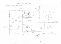
I noticed from looking at a images of other Kenwood KA 801 amps that some of the them had less components in the power amp stage than mine did and not only that they are shown in the service manual in the section displaying the foil tracks and component layout but they are not shown on the schematic.
I have scanned a pencil drawing that i have copied from the PCB layout a screen shot of the PCB and the service manual schmatic
The components not shown on the schematic are;
C2 (10uf,25v)
C4 (10uf,25v)
C6 (10uf,25v)
C14 (47uf,10)
D2
D4
R12 (27k)
R14 (27k)
Attachments
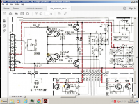
Q10,12 and Q6,8 form active current limiters which restrict the output of the power transistors to within their SOA limits. They are safety circuits incorporated in but not considered part of the power amplifier itself. Usually they require extensive field testing to ensure they work effectively without noticeably affecting the audio. It would seem like there was a problem there and it was addressed by those mods at some point in the model's production lifetime.
It's normal to see minor revisions to models but of course, if you weren't a service tech back then, you wouldn't receive updates. It's history though and the supporting documentation for many such ancient models is now unobtanium.
It's normal to see minor revisions to models but of course, if you weren't a service tech back then, you wouldn't receive updates. It's history though and the supporting documentation for many such ancient models is now unobtanium.
C2 is something I was surprised not to see on the original as bypassing the vbe generator (R + diode) is pretty standard practice and can help with high frequency performance/distortion, particularly with regard to ensuring the driver stage can turn 'off' quickly.
The R's and C's added to the current limiter modify the basic characteristic making it less prone to cut in to enthusiastically, perhaps when faced with a more challenging load such as a speaker with a reactive and low impedance.
The R's and C's added to the current limiter modify the basic characteristic making it less prone to cut in to enthusiastically, perhaps when faced with a more challenging load such as a speaker with a reactive and low impedance.
you have swapped your supply rails.Up date,
I noticed from looking at a images of other Kenwood KA 801 amps that some of the them had less components in the power amp stage than mine did and not only that they are shown in the service manual in the section displaying the foil tracks and component layout but they are not shown on the schematic.
I have scanned a pencil drawing that i have copied from the PCB layout a screen shot of the PCB and the service manual schmatic
The components not shown on the schematic are;
C2 (10uf,25v)
C4 (10uf,25v)
C6 (10uf,25v)
C14 (47uf,10)
D2
D4
R12 (27k)
R14 (27k)
The middle sch has -ve at the top, your version has +ve at the top.
- Status
- Not open for further replies.
- Home
- Amplifiers
- Solid State
- Output bias just keep keeps creeping up