Seeing as how interest in complementary diff pair input “symmetric” amps just won’t go away…
I’ve wasted a wet weekend day seeing if I could get my optoisolator bias scheme to sim
As many have (re)discovered for themselves, current mirror loads on complementary diff pairs don’t set the bias current in the VAS, the VAS needs its own bias setting feedback circuit
This sim shows a servo that senses the VAS bias current with a optoisolator LED in the “Vbe” multiplier, the current in the phototransistor collector-base diode is a fixed (small) ratio of the LED current – the cb-photodiode is working in “photovoltaic” mode with ~0 V across it giving highly accurate transfer of photo-current into the servo op amp virtual ground
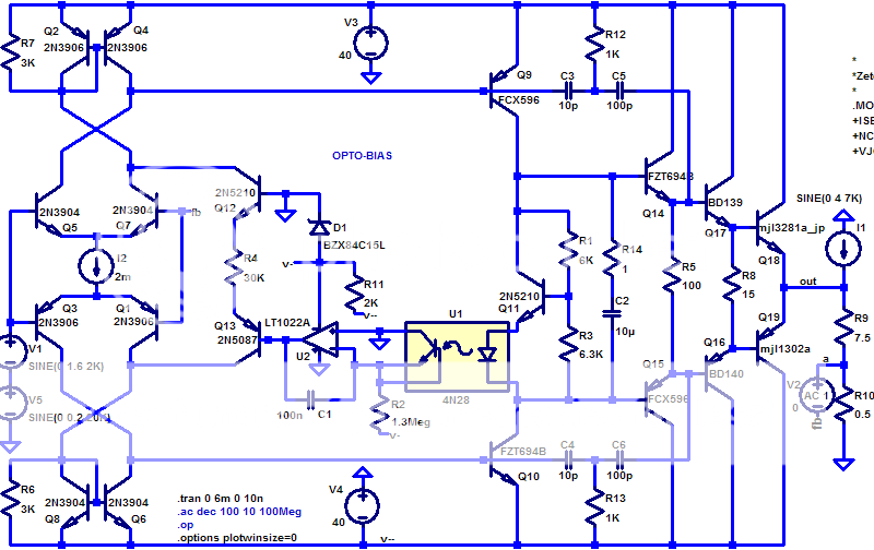
The fet input op amp controls a double-ended common mode current source Q12,13 which is connected to the current mirrors to control the VAS operating current, the servo balances the photodiode current against setpoint current in R2 – the ratio of R2 current to LED current should be very constant in this scheme but you will have to measure it for each optoisolator (I_R2= -1*I_photodiode)
To minimize parts I’ve relied on a fet op amp with input common mode range that can equal its V+ supply – this is true for real world TL071/LF351/LF411 and the LT spice model seems to work too (but not all fet op amps can do this)
This sim gives ~85 dB mid band loop gain and the 2 pole comp helps it hold up to 70 dB @ 20 KHz ( actually I’m only seeing ~ 10 dB more with the 2 pole comp ) - feedback from the tapped speaker load is just an entertaining spice hack, I'm pretty sure it doesn't effect the compensation more the sim's model accuracy limits
As usual, this is just a sim illustrating a circuit concept – not a debugged, properly dimensioned working circuit –needs start up and clipping behavior looked at as a minimum – and the output devices are not optimal, just what I’ve collected spice models for so far; you’ll have to change them to your own favorites
Simulated distortion components are ~ 100 dB below the 32 V test waveform peak, the test current source shows Zout ~ 50 uOhm @ 7 KHz (and at 4 A AC, and relatively prime freq ratio, it drags the output Q I-V all over the map, just like a complex speaker load, or “back EMF” for those preferring that language)
I’ve wasted a wet weekend day seeing if I could get my optoisolator bias scheme to sim
As many have (re)discovered for themselves, current mirror loads on complementary diff pairs don’t set the bias current in the VAS, the VAS needs its own bias setting feedback circuit
This sim shows a servo that senses the VAS bias current with a optoisolator LED in the “Vbe” multiplier, the current in the phototransistor collector-base diode is a fixed (small) ratio of the LED current – the cb-photodiode is working in “photovoltaic” mode with ~0 V across it giving highly accurate transfer of photo-current into the servo op amp virtual ground
The fet input op amp controls a double-ended common mode current source Q12,13 which is connected to the current mirrors to control the VAS operating current, the servo balances the photodiode current against setpoint current in R2 – the ratio of R2 current to LED current should be very constant in this scheme but you will have to measure it for each optoisolator (I_R2= -1*I_photodiode)
To minimize parts I’ve relied on a fet op amp with input common mode range that can equal its V+ supply – this is true for real world TL071/LF351/LF411 and the LT spice model seems to work too (but not all fet op amps can do this)
This sim gives ~85 dB mid band loop gain and the 2 pole comp helps it hold up to 70 dB @ 20 KHz ( actually I’m only seeing ~ 10 dB more with the 2 pole comp ) - feedback from the tapped speaker load is just an entertaining spice hack, I'm pretty sure it doesn't effect the compensation more the sim's model accuracy limits
As usual, this is just a sim illustrating a circuit concept – not a debugged, properly dimensioned working circuit –needs start up and clipping behavior looked at as a minimum – and the output devices are not optimal, just what I’ve collected spice models for so far; you’ll have to change them to your own favorites
Simulated distortion components are ~ 100 dB below the 32 V test waveform peak, the test current source shows Zout ~ 50 uOhm @ 7 KHz (and at 4 A AC, and relatively prime freq ratio, it drags the output Q I-V all over the map, just like a complex speaker load, or “back EMF” for those preferring that language)
Attachments
That's really nice. Do you think it would be worth the extra complication? Do you know of any other ways of fixing bias current?
A dozen components here, a dozen components there…
Resistor collector loads are simpler
But the idea of some extra parts to bias the amp doesn’t seem prohibitively complex
Current mirror collector loads can improve diff pair dc Ic bias balance, greatly improving their linearity – you can find amplifier schematics/sims here where poorly coordinated collector R load/VAS bias point have the diff pair Qs operating with > 10% Ic mismatch – trimming the diff pair bias for Ic balance really should be a part of the instructions for those amps
Current mirrors also enable high loop gain – an interest of mine if not everyone’s cup o’ tea
Besides the idea of a common mode loop running “inside” of the diff gain stages of the amp is just plain fun
as usual the attachement in the 1st post is a Lt SwCadIII circuit file, change .txt to .asc - you will need to add your own power device models
The VAS devices Q9,10 I tried in the 1st sim really suck, replacing them with cascodes 2n5210/bd139, 2n5087/bd140 with 2 V bias boosts gain and drops distortion to ridiculous levels; -140 dB (up c3,4 to 20p to get back to 60 degree phase margin)
(of course this could just mean the zetex models are more accurate…)
(of course this could just mean the zetex models are more accurate…)
jcx said:.........of course this could just mean the zetex models are more accurate…
They are....🙂
jcx,
I'm not sure I quite understand the configuration of the biased cascode, could you post an updated .asc file.
Cheers,
Jon
I'm not sure I quite understand the configuration of the biased cascode, could you post an updated .asc file.
Cheers,
Jon
I want to emphasize the symmetry improvement in actual operation by using current mirror collector loads compared to resistor loads with single ended output, even with good Ic balance
Current mirror differencing of both transistors’ collector currents reduces distortion from Zcb modulation with input common mode voltage swing – this cancellation between same type transistors within a mirror loaded diff pair reduces distortion much more than the cancellation between upper and lower diff pairs in the complementary diff input design which requires matching of npn to pnp parameters
My main point for this thread is the VAS bias servo which allows the use of current mirror loading in the complementary diff pair and the consequent improvement of input stage “symmetry” which so many complementary diff pair implementations with resistor collector loads are lacking
I’m reluctantly adding the cascode sim .asc file; cascode VAS has been discussed elsewhere here and the added gain and bias considerations can complicate clipping behavior – the sim only demonstrates that high gain/low distortion linear operation is possible, not that the topology is ready for the real world (you'll have to comment out the .load bais - the extra gain can make it difficult for spice to find the bias point if you crank the sim tolerances so I save a working bias point first )
Attachments
jcx said:I want to emphasize the symmetry improvement in actual operation by using current mirror collector loads compared to resistor loads with single ended output, even with good Ic balance
Current mirror differencing of both transistors’ collector currents reduces distortion from Zcb modulation with input common mode voltage swing – this cancellation between same type transistors within a mirror loaded diff pair reduces distortion much more than the cancellation between upper and lower diff pairs in the complementary diff input design which requires matching of npn to pnp parameters
My main point for this thread is the VAS bias servo which allows the use of current mirror loading in the complementary diff pair and the consequent improvement of input stage “symmetry” which so many complementary diff pair implementations with resistor collector loads are lacking
I’m reluctantly adding the cascode sim .asc file; cascode VAS has been discussed elsewhere here and the added gain and bias considerations can complicate clipping behavior – the sim only demonstrates that high gain/low distortion linear operation is possible, not that the topology is ready for the real world (you'll have to comment out the .load bais - the extra gain can make it difficult for spice to find the bias point if you crank the sim tolerances so I save a working bias point first )
Hi JCX,
Nice circuit, but i have few questions for you.
1] Have you simulated this circuit with signal input above 30kHz.
2] Is there any phase margin arises or phase lag occurs when driving with high frequency signal say 20kHz
3] Do you agree that this totpology cancels the distortion effects more than the traditional topologies.
regards
Kanwar
Go right ahead, Linear Technology’s SwCAD III spice simulator software is free from www.linear.com, even pretty compact (~ 3M last time I downloaded a complete new install)
I think the BD139/140 models were from Fairchild, on-semiconductor is the Motorola discrete spin off (but their spice models appear to have accuracy problems, maybe try Fairchild substitutes for pwr models too)
You can look at loop gain with V2 AC source in a .ac analysis, for what its worth given the modeling issues and .ac analysis incremental linearization of the amp about a not easily inspected bias point it determines with a different algorithm than in the .tran analysis – also this is still a “sketch” of an amp, realistic input and feedback impedance will introduce phase and distortion issues in the input stage, parallel output Qs are necessary and change high frequency loading, ect.
Phase margin will vary with different operating points and .tran is required to get at all close, looking at the ringing/settling of small, fast steps riding on a large low frequency sine or triangle is sometimes helpful – Iv’e not gone that far with this sim
Since there is ~70 dB loop gain @20KHz the maximum phase deviation from the ideal feedback determined response is ~0.03 degree ( from 90/3162) in this sim (even less with the cascode vas 2nd circuit)
I’m trying to say that I don’t think some complementary diff pairs with collector resistor load schematics I’ve seen here are much more than “eye candy” due to Ic imbalance and lack of cancellation of Zcb errors between right and left Q in each diff pair and the forlorn hope of useful top/bottom npn and pnp inter-diff pair distortion cancellations– there is the potential for some even order nonlinearity cancellation from differential drive of the VAS but that is possible in several other topologies as well (diff pair 2nd stage is another alternative that works with input diff pair collector resistor load)
Adding current mirror loads to the complementary diff pair increases distortion cancellation within each diff pair and increases gain available for negative feedback
Differential operation distortion cancellation is limited by device matching and odd order nonlinearities that don’t cancel so that it shouldn’t be relied on for more than 20-30 dB improvement, high negative feedback gain reduces distortion from both even and odd order nonlinearities but is most effective at low frequencies, while cancellation can work to much higher frequencies – there might be a reason diff pair input followed by large gain is the most common amp topology
- Status
- Not open for further replies.
- Home
- Amplifiers
- Solid State
- optoisolator VAS bias for Comp Diff?