Not quite optimal decoupling!
Maybe price is an influencing factor! A Rubycon ZA and ceramic to bypass is 20% of the cost of an OsCon SH.
In Guido's article, he talks about placing the decoupling cap directly between the supply pin and the ground pin of an IC - and not using a ceramic for bypassing.
Does this change when the electolytic cannot be optimally positioned (across these pins)?
Should the electrolytic then be positioned as close as possible to the supply pin with its other lead connected directly to the ground plane (not through a trace)?
In this case, is it beneficial to use a ceramic between the supply and ground pins?
Oli said:I had read Guido's words of knowledge, but I lacked confidence in applying what they were telling me. Indeed, Sanyo give PDF examples on their website where OsCons alone are used as decoupling devices.
So why do so many people believe in using ceramics and low impedance electrolytics in parallel? Are they simply wrong?
Maybe price is an influencing factor! A Rubycon ZA and ceramic to bypass is 20% of the cost of an OsCon SH.
In Guido's article, he talks about placing the decoupling cap directly between the supply pin and the ground pin of an IC - and not using a ceramic for bypassing.
Does this change when the electolytic cannot be optimally positioned (across these pins)?
Should the electrolytic then be positioned as close as possible to the supply pin with its other lead connected directly to the ground plane (not through a trace)?
In this case, is it beneficial to use a ceramic between the supply and ground pins?
The decoupling capacitor shall always be connected very close to the supply pin and directly to the groundplane. Any PCB trace degrade the function, it can be viewed as increase of capacitor ESL.
The problem when using two caps in parallel is that you create a parallel resonance circuit since the capacitor contains inductance. The resonance is dampened by the capacitor resistance but with a low ESR lytics and a ceramic there's not much of damping.
A series resistance between the two capacitors can be used but have to be sized with allot of care.
This decoupling ringing is however very narrow-banded and I'm not sure of how much problems they really induce. It should be very implementation dependent.
OsCon is a good capacitor no doubt and can be used as a single decoupling capacitor were you don't except very high frequencies. I've used them this way with success, I've also used the lythic - ceramics combo with success.
I prefer I using the lythic - ceramics combo but keep the potential ringing problem in mind, preferably measuring at the supply pin and changing the capacitor sizes in case of problems.
I usually have the lytic placed some distance apart from the ceramic, mostly of practical reasons. This also increases the impedance between the two and dampens the ringing. However, if the trace is too long it can degrade bypass function and increase EMI problems.
One shall also remember that the lythic is not allways need and can therefor give more problems than it solves.
/Jesper
jesper said:The decoupling capacitor shall always be connected very close to the supply pin and directly to the groundplane. Any PCB trace degrade the function, it can be viewed as increase of capacitor ESL.
The problem when using two caps in parallel is that you create a parallel resonance circuit since the capacitor contains inductance. The resonance is dampened by the capacitor resistance but with a low ESR lytics and a ceramic there's not much of damping.
A series resistance between the two capacitors can be used but have to be sized with allot of care.
I agree here...
I usually have the lytic placed some distance apart from the ceramic, mostly of practical reasons. This also increases the impedance between the two and dampens the ringing. However, if the trace is too long it can degrade bypass function and increase EMI problems.
but not here... Seems to be a contradiction, huh ? Additionnal trace lengths do not provide damping (resistance), but just add inductance... No ?
Thanks for your reply Jesper.
In my application, I am moddifying an existing circuit rather than designing a new one. The electrolytic is placed quite close to the supply pin and connected to the ground plane by a trace. There is a SMD ceramic in parallel. What is the best way to improve this arrangement:
1. Connect the ground pin of the electrolytic directly to the ground plane with a short link through the PCB?
2. Remove the SMD ceramic or leave it in place?
3. Add a ceramic cap across the the supply and ground pins of the chip?
PS. I do not have measuring equipment (only a multimeter), so I'm looking for the most reliable solution.
but not here... Seems to be a contradiction, huh ? Additionnal trace lengths do not provide damping (resistance), but just add inductance... No ? [/B][/QUOTE]
CheffDeGaar:
You're right, didn't finish thinking there, the increase in inductance will dominate. Placing them close together will increase bypassing performance at lower frequencies.
I distance them apart for purely practical reasons..
/Jesper
CheffDeGaar:
You're right, didn't finish thinking there, the increase in inductance will dominate. Placing them close together will increase bypassing performance at lower frequencies.
I distance them apart for purely practical reasons..
/Jesper
1) The ringing between two parallel caps can be got rid of by introducing damping resistors. They don't need to take up a lot of space if they are SMTs. Measuring the resonance Q is a bit tricky at the frequencies involved, though. However, provided one is blessed with reasonably good data, calculations may go a long way.
2) Lex Kirchoff has been frequently invoked in this thread. When pondering about circuits clocked at 100 MHz electromagnetic theory is probably more useful than classical lumped element circuit theory. So when a gate switches state we really ought to consider the propagation of the EM-wave and think in terms of the Poynting vector S = ExB/mu and consider the PCB tracks and planes only as "rails" for the EM-field.
2) Lex Kirchoff has been frequently invoked in this thread. When pondering about circuits clocked at 100 MHz electromagnetic theory is probably more useful than classical lumped element circuit theory. So when a gate switches state we really ought to consider the propagation of the EM-wave and think in terms of the Poynting vector S = ExB/mu and consider the PCB tracks and planes only as "rails" for the EM-field.
Hi Bolinder,
you are probably right. I think one of the problems here is also that some think that DAC's are digital circuits, have no experience with other digital circuits, and think that everything that is good for DAC's should be used in any digital design, regardless of clock frequency.
Best regards,
Jaka Racman
Bolinder said:2) Lex Kirchoff has been frequently invoked in this thread. When pondering about circuits clocked at 100 MHz electromagnetic theory is probably more useful than classical lumped element circuit theory. So when a gate switches state we really ought to consider the propagation of the EM-wave and think in terms of the Poynting vector S = ExB/mu and consider the PCB tracks and planes only as "rails" for the EM-field.
Well, depends... Wavelenght @ 100MHz is 3 meters in air, and about 1.5 meter in FR4. For fast transients (square signals), even considering the 20th harmonic leads to 15cm wavelenth in air (7.5cm in FR4). Propagative problems are not an issue here when speaking of supply lines and decoupling networks, and Kirchoff still rules, provided the decoupling caps are not 10 feet away 😉. If traces have to be short, it's more regarding their intrinsic inductance.
EM coupling has also to be addressed (EM leakage from active PCB traces -ie cloks- onto supply lines), but has just to be considered as an external noise source, and has very little influence on the impedance of the decoupling network.
Just my $0.02
Bolinder said:1) The ringing between two parallel caps can be got rid of by introducing damping resistors. They don't need to take up a lot of space if they are SMTs. Measuring the resonance Q is a bit tricky at the frequencies involved, though. However, provided one is blessed with reasonably good data, calculations may go a long way.
2) Lex Kirchoff has been frequently invoked in this thread. When pondering about circuits clocked at 100 MHz electromagnetic theory is probably more useful than classical lumped element circuit theory. So when a gate switches state we really ought to consider the propagation of the EM-wave and think in terms of the Poynting vector S = ExB/mu and consider the PCB tracks and planes only as "rails" for the EM-field.
Hi
I fully agree on your statement, but would like to place one remark
lumped element theory can still be used as long as the physical circuit (layout) is electrically short
If possible, I use lumped elements as it gives much more and quick insight in problems
cheers
Fin said:In my application, I am moddifying an existing circuit rather than designing a new one. The electrolytic is placed quite close to the supply pin and connected to the ground plane by a trace. There is a SMD ceramic in parallel. What is the best way to improve this arrangement:
1. Connect the ground pin of the electrolytic directly to the ground plane with a short link through the PCB?
2. Remove the SMD ceramic or leave it in place?
3. Add a ceramic cap across the the supply and ground pins of the chip?
Anyone???
lumped element theory can still be used as long as the physical circuit (layout) is electrically short If possible, I use lumped elements as it gives much more and quick insight in problems
Yes, it depends on the ratio rise-time / physical size and lumped element analysis is certainly easier. Although magnetic and electric interference may also be modelled as mutual inductances and capacitances, respectively, I still find it useful to try to build a mental picture of how the EM-field propagates. Of cause, the two methods are not mutually exclusive and keeping booth in mind does no harm.
Konnichiwa,
In short, first buy at least a decent 'scope, or you have little business of poking around in high speed digital circuits.
Secondly, the most reliable methode I am aware of involves the use of at least THREE capacitors in parallel at the local PSU node in IC's. The capacitors should have a similar ESR and two of them are best realised as 0805 Format SMD's, namely 10nF/X7R and 100nF/Z5U or Y5U (the X7R/Z5U/Y5U are dielectrics), the third is best realised as moderate value, low inductance electrolytic capcitor, such as Sanyo Os-Con, as said, with an ESR similar to that of the two SMD ceramic capacitors.
Usually such a triplet shows minimal and low Q spikes in the impedance plot, the biggest limit in this arrangement, if applied correctly, tends to be the lead inductance of the IC itself.
Sayonara
Fin said:In my application, I am moddifying an existing circuit rather than designing a new one. The electrolytic is placed quite close to the supply pin and connected to the ground plane by a trace. There is a SMD ceramic in parallel. What is the best way to improve this arrangement:
1. Connect the ground pin of the electrolytic directly to the ground plane with a short link through the PCB?
2. Remove the SMD ceramic or leave it in place?
3. Add a ceramic cap across the the supply and ground pins of the chip?
PS. I do not have measuring equipment (only a multimeter), so I'm looking for the most reliable solution.
In short, first buy at least a decent 'scope, or you have little business of poking around in high speed digital circuits.
Secondly, the most reliable methode I am aware of involves the use of at least THREE capacitors in parallel at the local PSU node in IC's. The capacitors should have a similar ESR and two of them are best realised as 0805 Format SMD's, namely 10nF/X7R and 100nF/Z5U or Y5U (the X7R/Z5U/Y5U are dielectrics), the third is best realised as moderate value, low inductance electrolytic capcitor, such as Sanyo Os-Con, as said, with an ESR similar to that of the two SMD ceramic capacitors.
Usually such a triplet shows minimal and low Q spikes in the impedance plot, the biggest limit in this arrangement, if applied correctly, tends to be the lead inductance of the IC itself.
Sayonara
Kuei Yang Wang,
Yep that the ticket when you dealing with HF noise on the power supply lines. If you have a very low noise supply and a low impedance ground returns you might not have to go to all that trouble, however you want really know till it's build of course unless you dealing with ALS, 4000 series CMOS Digital.
Yep that the ticket when you dealing with HF noise on the power supply lines. If you have a very low noise supply and a low impedance ground returns you might not have to go to all that trouble, however you want really know till it's build of course unless you dealing with ALS, 4000 series CMOS Digital.
Hi Thorsten - thanks for your help here.
Maybe I could install some appropriate cards in my computer.
I think where some of us are getting confused is in knowing when to apply the the above layout or either of the following descriptions:
Does it come down to how close you can get the electrolytic to the supply and ground pins?
For instance, if you can position the electrolytic directly across the pins, then it may be possible to dispense with the ceramics. However, if you cannot achieve this, then bypassing with additional ceramics is better?
Maybe I'm looking for an answer that is too simple or does not exist.
Originally posted by Kuei Yang Wang
In short, first buy at least a decent 'scope, or you have little business of poking around in high speed digital circuits.
Maybe I could install some appropriate cards in my computer.
Originally posted by Kuei Yang Wang
Secondly, the most reliable methode I am aware of involves the use of at least THREE capacitors in parallel at the local PSU node in IC's. The capacitors should have a similar ESR and two of them are best realised as 0805 Format SMD's, namely 10nF/X7R and 100nF/Z5U or Y5U (the X7R/Z5U/Y5U are dielectrics), the third is best realised as moderate value, low inductance electrolytic capcitor, such as Sanyo Os-Con, as said, with an ESR similar to that of the two SMD ceramic capacitors.
I think where some of us are getting confused is in knowing when to apply the the above layout or either of the following descriptions:
From Guido Tent's Article:- Supply decoupling and layout of circuits with digital ICs
Very often two capacitors are connected in parallel; 100 nF ceramic and 4,7 mF for example. This habit originates from history. In the early years electrolytics had poor RF characteristics
and a smaller ceramic or foil cap, with good RF behaviour, was placed in parallel.
Modern electrolytics are far better RF performers. Their construction is such that the series inductance is very low (both films are terminated at the same side). They have very low
impedance over up to 4 decades in frequency; Enough to say goodbye to the additional ceramic capacitor. It saves money and space as well and eliminates the risk of yet another
resonance.
From TNT article.
Andy Groove (Mr. Ankoru) from Audio Note UK says that the Black Gate PK Series of Capacitors works well. Similar to Nichicon PL-Series / 1206-Ceramic Combination, the Black Gates are effective to over 100MHz on their own.
This of Course will only work if You can keep the inductance from the Leads and the PCB-Tracks low. Thus these Cap's would be placed best with ultra-short leads below the PCB. The Black Gate PK Series also seems to be limited to values of maximally 47uF.
Does it come down to how close you can get the electrolytic to the supply and ground pins?
For instance, if you can position the electrolytic directly across the pins, then it may be possible to dispense with the ceramics. However, if you cannot achieve this, then bypassing with additional ceramics is better?
Maybe I'm looking for an answer that is too simple or does not exist.
A PCB; not Swiss cheese!
Here's a question fielded at Guido Tent, but all contributions are most welcome... 🙂
Overview
-----------
- I am designing the PCB for my DAC (see this thread for details).
- I am applying Guido Tent's single ground plane philosophy 😀
- I am using a dual layer PCB with the top layer forming the ground plane.
- The bottom layer of the PCB will contain lots of signal lines, power lines, analogue etc.
The Question (I have a vague idea, but I would like confirmation)
----------------
I intend to copper pour fill remaining gaps on the back side of the PCB and ground these islands.
I vaguely remember something about unterminated ground islands acting as r.f. radiators- am I correct?
My gut feeling is that it is okay to adopt the aforementioned approach as long as the top and bottom ground planes are connected regularly with vias, but how extreme do I go? I want a PCB, not swiss cheese!
or..... is this a bad idea all together?
OLI
It either at ground potential or it not, you know 0 volts. Daisy chained ground can radiate
Be sure to keep you ground plane runs as wide as possible and remember that you can connect grounds with jumpers or as I call them zero ohm resistors. That mean you can have multiple grounds area or a single one.
I stick with multiple ground planes I was taught at Texas Instruments
Also, as was pointed out that surface mount components don't suffer the severe problems as standard dual inline components.
jewilson said:OLI
It either at ground potential or it not, you know 0 volts. Daisy chained ground can radiate
only if current runs through them
regards
So Guido,
your saying that you promote the implementation of daisy chaining circuits when grounding. Is that correct!
your saying that you promote the implementation of daisy chaining circuits when grounding. Is that correct!
jewilson said:So Guido,
your saying that you promote the implementation of daisy chaining circuits when grounding. Is that correct!
No, that is not what I wrote:
I do not promote that, but I stated that you may do so, without being punished by EMI or signal integrity problems,
under the assumption that no RF currents run through the plane
regards
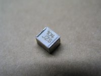
Hi all,
let me share a little opinions.
I also design PCB for diyer kits.
recently I collect some capacitors sample for the supplier.
I had only 100pcs on hand but I test very good.
pls take a look for the decouple cap for my kits.
my PCB.
http://www.diyaudio.com/forums/showthread.php?s=&postid=437051#post437051
this is the spec of the new sample decouple caps.
very good in digital interface use.
http://www.evox-rifa.com/cap_catalog/smdfilmc/smc.pdf
photos of the cap.
thanks
thomas
Attachments
- Status
- Not open for further replies.
- Home
- Source & Line
- Digital Source
- Optimum Decoupling of Digital ICs