Hello all,
I am just trying to understand what is going on in my very simple amplifier.
I am following a post on the internet.
Class B audio amplifier : ANALOG INTEGRATED CIRCUITS
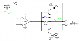
So I got to the first schematic and i added a buffer at the input.

And measuring the output with my oscilloscope gave me a nice output with no load. Blue is output. Red is input.

But once I placed a load over the output things became a little fuzzy.
I was expecting to see the cross-over distortion but I got more than I asked for.
Load is 220 Ohm. Blue is output. Red is input.

Why does my input distort when power is applied?
The supply voltage is +/-12V and the current draw for both supplies is 4mA.
Input signal is 500Hz 5Vpp or 1,77 VRMS from my function generator and the gain is set to about 1.
Thank you for any input or clarification!
X
I am just trying to understand what is going on in my very simple amplifier.
I am following a post on the internet.
Class B audio amplifier : ANALOG INTEGRATED CIRCUITS
So I got to the first schematic and i added a buffer at the input.
And measuring the output with my oscilloscope gave me a nice output with no load. Blue is output. Red is input.
But once I placed a load over the output things became a little fuzzy.
I was expecting to see the cross-over distortion but I got more than I asked for.
Load is 220 Ohm. Blue is output. Red is input.
Why does my input distort when power is applied?
The supply voltage is +/-12V and the current draw for both supplies is 4mA.
Input signal is 500Hz 5Vpp or 1,77 VRMS from my function generator and the gain is set to about 1.
Thank you for any input or clarification!
X
Try adding a little series resistance between the opamp output and the transistors (say 39 or 47 ohm). Also make sure the opamp is decoupled correctly across the supply pins and that the load returns to the correct ground point.
In addition to what Mooly said, I would also suggest following the layout suggested in the article (if you don't have protoboard, use pieces of stripboard), which seems to be bench-tested. Simplify from there. Remember, the layout is the circuit. Also recheck for any bad connections.
Hello all,
I am just trying to understand what is going on in my very simple amplifier.
I am following a post on the internet.
Class B audio amplifier : ANALOG INTEGRATED CIRCUITS
So I got to the first schematic and i added a buffer at the input.
View attachment 786427
And measuring the output with my oscilloscope gave me a nice output with no load. Blue is output. Red is input.
View attachment 786428
But once I placed a load over the output things became a little fuzzy.
I was expecting to see the cross-over distortion but I got more than I asked for.
Load is 220 Ohm. Blue is output. Red is input.
View attachment 786429
Why does my input distort when power is applied?
The supply voltage is +/-12V and the current draw for both supplies is 4mA.
Input signal is 500Hz 5Vpp or 1,77 VRMS from my function generator and the gain is set to about 1.
Thank you for any input or clarification!
X
Your output stage is off at the zero crossing, because there is no Vbe at that point to drive the output transistors. That is why there is a flat portion in the output near zero signal with load. So the output of the opamp has to 'jump' from one base Vbe to another through the zero crossing. It can do that with no load, but not with load.
It will get better if you take the feedback from the output instead of from the opamp output, but it will not completely go away, unless you make sure that there is always a bit of current through those output transistors.
That is called quiescent bias current and a pair of diodes and some resistors are involved, there's lots of Google hits for it.
Jan
As a thought... + a revised thought
Attachments


Last edited:
Hi guys,
Thank you for all the replies. A very active forum!
I am on my mobile for the moment. Once I get home I will try out your ideas and report back.
I have some understanding of amplifiers and I know that a class b output stage will produce x-over distortion. I just didn't quite understand why my input also got distorted with the output. It seemed so simple! ��
Thanks again!
X
Try it like this.
With an opamp with more output drive the 150Ω can be smaller (down to 50Ω) and better results.
Mona
With an opamp with more output drive the 150Ω can be smaller (down to 50Ω) and better results.
Mona
Attachments
Last edited:
Hi guys,
Thank you for all the replies. A very active forum!
I am on my mobile for the moment. Once I get home I will try out your ideas and report back.
I have some understanding of amplifiers and I know that a class b output stage will produce x-over distortion. I just didn't quite understand why my input also got distorted with the output. It seemed so simple! ��
Thanks again!
X
The reason for that might be that you are feeding the circuit from a source that has appreciable output resistance. The distorted signal on the feedback chain then divides across all the impedances, and can appear at the opamp input, but not directly at your source output. Did you check that?
Edit: if you say 'distortion at the input' did you mean the opamp input pin?
Jan
The reason for that might be...
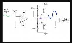
I think my second revision example graphic demonstrates the right way to accomplish a nearly-distortion-free class “b” output BJT stage hooked to the op-amp of the OP's first post.
Would love to hear otherwise if you think so!
Really!!!
Just Saying,
GoatGuy ✓
Attachments
Last edited:
Try it like this....Mona
I'll ask you too, Mona… don't you think that the continuous bias and small-signal diode lifter approach circumvents the crossover distortion business easily? Take a look just above.
The problem with that is the resistor drive of the output transistors.The more current in the speaker the less base current available.I'll ask you too, Mona… don't you think that the continuous bias and small-signal diode lifter approach circumvents the crossover distortion business easily? Take a look just above.
It could function with CCS for the resistors but that makes the hole thing more complex.
With a low resistance between opamp-out and output, the amp is classA for small signals.The moment the voltage drop become greater then Vbe the transistors take over.
Mona
You simplified the original circuit and now you wonder why things go bad😀Hello all,
I am just trying to understand what is going on in my very simple amplifier.
I am following a post on the internet.
Class B audio amplifier : ANALOG INTEGRATED CIRCUITS
So I got to the first schematic and i added a buffer at the input.
View attachment 786427
And measuring the output with my oscilloscope gave me a nice output with no load. Blue is output. Red is input.
View attachment 786428
But once I placed a load over the output things became a little fuzzy.
I was expecting to see the cross-over distortion but I got more than I asked for.
Load is 220 Ohm. Blue is output. Red is input.
View attachment 786429
Why does my input distort when power is applied?
The supply voltage is +/-12V and the current draw for both supplies is 4mA.
Input signal is 500Hz 5Vpp or 1,77 VRMS from my function generator and the gain is set to about 1.
Thank you for any input or clarification!
X
The problem with that is the resistor drive of the output transistors.The more current in the speaker the less base current available. It could function with CCS for the resistors but that makes the hole thing more complex. With a low resistance between opamp-out and output, the amp is classA for small signals.The moment the voltage drop become greater then Vbe the transistors take over. Mona
I see… yes, I get it, and why you advised the possibility of using a lower series resistance than 150 Ω if there were more current drive to be had from the output of the op-amp. Nice.
But it seems to “run counter” to the little speaker-icon shown on the diagram.
To me, below VBE = 700 mV, there's a 150 Ω resistor in series with the 8 Ω speaker. Since it is a nice Kirchoff's Law current loop below 700 mV, ¹⁵⁰⁄₁₅₈ (95%) of the power is dissipated in the 150 Ω resistor, and ⁸⁄₁₅₈ or about 5% is for the speaker. Until cut-over.
If that dynamic analysis is right, then you have the same “cross-over distortion”, expressed a different way. 5% power until 700 mV of output, then way more power thereafter.
Again … doesn't my {2 resistor, 2 diode, feedback from output to negative input} kind of deal with all that in a much lower output impedance regime? I'll preëmptively grant that “22 kΩ” is likely too high a value, since we don't know the hFE of the output complimentary pair. But just pulling “numbers out of the usual hat”, one might expect hFE of oh, 100 or so, right? And a power supply what of +12, 0, –12 volts? Something convenient.
Then, at maximum positive excursion (VCC - 1 V sub-rail = 11 V), with VBE = 0.7 V too … the output is 10.3 V or thereabouts. Into 8 … no, let's say 4 Ω load
E = IR
I = E/R
… = 10.3 ÷ 4
… = 2.6 A
Work with that, divided by hFEI = E/R
… = 10.3 ÷ 4
… = 2.6 A
IB = IC / hFE …
… = 2.6 A ÷ 100 hFE
… = 26 mA
We certainly don't need IC that high as the quiescent current. Maybe only ¼ to ⅛ that level, or 3 to 6 mA into the base of each complimentary output transistor. … = 2.6 A ÷ 100 hFE
… = 26 mA
E = IR
R = E/I
… = 12 / (0.003 to 0.006)
… = 2,000 to 4,000 Ω
So there are the “better values” for the pair of resistors. Anything between would be fine. Of course, dependent on the hFE. Indeed: learning the hFE of each transistor would determine the actual value of each ballast resistor. They don't need (and really shouldn't be expected) to be the same!R = E/I
… = 12 / (0.003 to 0.006)
… = 2,000 to 4,000 Ω
As always, good hearing your input, Mona.
GoatGuy ✓
Hello all !
Once i got home I started trying out all your suggestions. I started with the first one and Bingo! Thank you Mooly, I decoupled the OPAMP at its power supplies and the distortion was gone. I now get the distortion I was looking for !

I will continue with the rest of the schematics I see you guys posted. See how far I can take this little experiment.
@UltimateX86 Thanks for the link, going to be a good read
@jan Yes I did mean the OPAMP input pin. Thanks for the info I will be sure to check that stuff out before posting about an error like this again.
@GoatGuy I will test your schematic and post the results here. Thank you!
@Ketje Thanks for the schematic but I think GoatGuy's will prove better for the next experiment. Merci Ket !
X
Once i got home I started trying out all your suggestions. I started with the first one and Bingo! Thank you Mooly, I decoupled the OPAMP at its power supplies and the distortion was gone. I now get the distortion I was looking for !
I will continue with the rest of the schematics I see you guys posted. See how far I can take this little experiment.
@UltimateX86 Thanks for the link, going to be a good read
@jan Yes I did mean the OPAMP input pin. Thanks for the info I will be sure to check that stuff out before posting about an error like this again.
@GoatGuy I will test your schematic and post the results here. Thank you!
@Ketje Thanks for the schematic but I think GoatGuy's will prove better for the next experiment. Merci Ket !
X
Goatguy, I was commenting on the input distortion he was seeing.
I was also asking where he measured that input distortion - at the end of the pot, or at the opamp input.
Jan
I was also asking where he measured that input distortion - at the end of the pot, or at the opamp input.
Jan
Goatguy, I was commenting on the input distortion he was seeing. I was also asking where he measured that input distortion - at the end of the pot, or at the opamp input. Jan
Ah, what a difference a prefix makes! input vs output. Thx. I hope to get feedback from OP re: his trial(s) of various topologies… It reminds me of my mis-spent youth.
LOL
GoatGuy ✓
Lots of work today. Will post tommorow. Before I posted my last message I hadn't seen all the new posts , interesting stuff. Looking forward to get busy.
X
X
Hi guys,
An update :
I've been experimenting with GoatGuy's suggestion. The 22K resistor was as said too high. 3K seemed to work at lower output levels.
A few pro's and contra's of GoatGuy's schematic against the simple class-b output with feedback:
High freq response is a lot better in GoatGuy's schematic, the simple schematic shows "ringing" (if that's the right word for it).

Output is a little "fuzzy" in GoatGuys schematic compared to the simple schematic. This could be because of my breadboard maybe ?

What I understand to be thermal runaway happens with GoatGuy's schematic. Transistors where heating up and Ic was rising fast because of it. I placed the diodes in the heat-sink(small heat-sink) to try and compensate.
The simple design also warmed up but stayed at a constant 56°C while the Ic didn't change.
So when i fix the thermal problem and the fuzzy output, I think it could be a good base to go further on.
A little extra question:
Would the ringing with the simple schematic go away if the OPAMP had a higher slew-rate? Here is a picture of the OPAMP output vs the transistor output at low and high freq. Interesting stuff ! 😉
Low freq

High freq

Again thank you all!
PS: Ketje, i'll try your scheme next.
Xa4
An update :
I've been experimenting with GoatGuy's suggestion. The 22K resistor was as said too high. 3K seemed to work at lower output levels.
A few pro's and contra's of GoatGuy's schematic against the simple class-b output with feedback:
High freq response is a lot better in GoatGuy's schematic, the simple schematic shows "ringing" (if that's the right word for it).
Output is a little "fuzzy" in GoatGuys schematic compared to the simple schematic. This could be because of my breadboard maybe ?
What I understand to be thermal runaway happens with GoatGuy's schematic. Transistors where heating up and Ic was rising fast because of it. I placed the diodes in the heat-sink(small heat-sink) to try and compensate.
The simple design also warmed up but stayed at a constant 56°C while the Ic didn't change.
So when i fix the thermal problem and the fuzzy output, I think it could be a good base to go further on.
A little extra question:
Would the ringing with the simple schematic go away if the OPAMP had a higher slew-rate? Here is a picture of the OPAMP output vs the transistor output at low and high freq. Interesting stuff ! 😉
Low freq
High freq
Again thank you all!
PS: Ketje, i'll try your scheme next.
Xa4
- Home
- Amplifiers
- Solid State
- Opamp with Class B output stage distortion