Hi all!
The further i dig on it, more doubts arise...¿is there a RIGHT way to trace the power traces on a pcb for dual opamps?.
¿should these traces be separated by gnd on the top layer? or as close as possible of each other? or should i get rid of the thin gnd in between the two power traces on the top layer? Considering always that i have a bottom layer gnd plane uncut below any trace of the top layer.
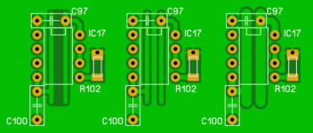
attached is a picture with 3 layouts. don't pay attention about the smd capacitor..is there because i usually use one side of dual opamps..
My application is small signal audio design. 0.775v, not power amplifier.
I usually route my power tracks as the layout depicted in the center.( the second from left to right) but i sometimes saw the third layout with the thickest traces in some boards.
As a side question, i usually try to orient the gnd pin of the bypass capacitors to the OUTPUT of the opamp, as mentioned in many app notes...¿i'm right?
Thanks for your help!
JAY X
The further i dig on it, more doubts arise...¿is there a RIGHT way to trace the power traces on a pcb for dual opamps?.
¿should these traces be separated by gnd on the top layer? or as close as possible of each other? or should i get rid of the thin gnd in between the two power traces on the top layer? Considering always that i have a bottom layer gnd plane uncut below any trace of the top layer.
attached is a picture with 3 layouts. don't pay attention about the smd capacitor..is there because i usually use one side of dual opamps..
My application is small signal audio design. 0.775v, not power amplifier.
I usually route my power tracks as the layout depicted in the center.( the second from left to right) but i sometimes saw the third layout with the thickest traces in some boards.
As a side question, i usually try to orient the gnd pin of the bypass capacitors to the OUTPUT of the opamp, as mentioned in many app notes...¿i'm right?
Thanks for your help!
JAY X
Attachments
Hi!
what is the effect of having the power traces close together? In soic8 packages with 0.8mm trace thickness, traces are close together but not touching...¿is there as negative effect? or in dual supply opamps it is beneficial?
Jay x
what is the effect of having the power traces close together? In soic8 packages with 0.8mm trace thickness, traces are close together but not touching...¿is there as negative effect? or in dual supply opamps it is beneficial?
Jay x
The power supply sends DC to the audio circuit, but this circuit tries to convert some of this DC into radio frequency noise. So we need a low impedance radio frequency path back to the power supply so that the supply can fight this noise. The closer that the traces are, the lower the impedance of this path.
Sorry for the late reply, but the middle version is probably best. It will keep the long bus traces lower inductance, but you'll have to run a field solver to give you the parasitics. At the end of the day, if the opamp is a low current and your output current is not heavy, I don't think you'll see any significant difference. It may be more important to pick the right decoupling cap, the correct value and proper rating (x7r if ceramic).
from Marce's sloa069 link
Now do you believe me?
I knew I had seen the vertically stacked multiplate capacitor somewhere.Fortunately, there is a very easy way to eliminate PRF1, as well as all odd parallel resonant
frequencies. If the capacitor is mounted on its side, the plates inside the capacitor are now
perpendicular to the PCB:
Figure 7. Vertical Capacitor Mounting
This will eliminate the parasitic capacitances between the plates of the capacitor and planes on
the PCB. The resulting spectrum shows that PRF1, as well as all odd parallel resonances, are
eliminated:
Now do you believe me?
Problem is how caps come on the tape, generally horizontal... for DIY Audio will you notice a difference...
Solution to what though, its not going to make any difference in the world of audio. Why look for solutions to problems that don't have any effect, just following the generic basic decoupling rules are enough, try getting that correct first instead of worrying about things that you may have to address if you are working in microwave frequency range... They have deliberately left of the scale because the actual levels depend on so many things, also as stated the cap is no good at decoupling at the parallel self res. frequencies... if you are having to worry about decoupling at 1.5GHz and above in Audio then there is something to worry about!
Never mind trying to get a decent solder joint to the cap with it on its side.
Never mind trying to get a decent solder joint to the cap with it on its side.
- Status
- Not open for further replies.
- Home
- Design & Build
- Construction Tips
- opamp power traces routing