Hi !
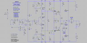
I am working on this schematics... It's just an opamp buffered with a diamond buffer.
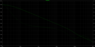
I need you guys help me to adjust the compensations, because I'm not good at this. I just tried some values until the phase margin looks good. But I don't know if this is how should be done. It seems that C11 (10pF) is the most important. Without it, the amplifier is not stable. But it also increase THD a little...
What is the DC-offset on output?
R3 at input is 33 kOhm
R5 at feedback is 10 kOhm.
We would expect both have same value for minimum offset.
R3 at input is 33 kOhm
R5 at feedback is 10 kOhm.
We would expect both have same value for minimum offset.
I am updating my LTSpice (I use MC normally). However, in the mean time, feedback output point OUT must be taken before the L1 (//R17) output inductor. As you have it, the L1 would NOT isolate the load capacitance, which is the reason why you need the L1. Then, loop gain stability (phase and gain margin) is to be analysed. Not the open loop gain plots.Here it is the archive with the .asc schematics and the models used...
feedback output point OUT must be taken before the L1
My god ! What a big mistake I did ! Thanks for pointing out !
I normally do not work with LTSpice and I have had issues with your models in my old LTSpice setup. However, I have changed some parts to make it working for me.Thanks for pointing out !
Below is the schematics

Do not look at the changes, they are unimportant for now. What you need is to investigate the loop gain. Here is the hint:
- you disconnect the generator from the input and connect it between the "Out" and new "a1" node.
- then you will run AC analysis and change the observed variable from "V(out)" to "V(out)/V(a1)"
- you will find the point where the magnitude plot (below) crosses 0dB line and at this point you will read phase angle. You can see you have about 65° phase margin even with the capacitive load 1u. That is good, the circuit is stable. It is also stable when capacitance is made zero.
- now, try this procedure in your simulator with your components.

now, try this procedure in your simulator with your components.
But I already did this... See the second picture from the initial post...
Here is it again, but without those 2 x 10pF caps. As you can see, there is no phase margin left...
Sorry for the confusion...
I was measuring the Bode plot like this, and then I just plot the output voltage (before the coild), without the need for division...

I was measuring the Bode plot like this, and then I just plot the output voltage (before the coild), without the need for division...
So, how does the loop gain look now, when you corrected the feedback output point? For stability, it is crucial to investigate the loop gain, not the transfer function from input to output. Loop gain, as the name indicates, is the transfer of the feedback loop.
All transistors need to thermal track in diamond buffer, it is the whole point.
How this is done with surface mount transistors not sure.
There is no thermal tracking for bias.
Many things can also be removed.
Typically use TO-126 folded drivers and emitter followers to thermal track.
R11 and R15 resistors can be used to set bias for the additional drop needed for Darlington.
Same thing no thermal compensation, typical to use diodes which need too thermal track outputs.
Or easier again to use TO-126 transistor as diodes and then will thermal track on heatsink
So, how does the loop gain look now, when you corrected the feedback output point?
There is no change. The phase margin is about 90 degrees, as before.
I'm happy with it, but I don't know if what I did there with C11, R18, R1, C10 is ok...
How this is done with surface mount transistors not sure.
I will put them close on PCB...
However, I have changed some parts to make it working for me.
OP is using LM4562 = 55 MHz
LT1122 = 14 MHz
So would be a completely different animal to stabilize.
Last edited:
How will you thermal track the outputs, the whole point of diamond buffer.I will put them close on PCB...
Resistors used for the second drop of the Darlington's are also not compensated for.
Would have to sim with 4562
R1 C10 likely just removed and C4 and C14 speedup capacitor not needed
Curious What is THD at almost full power at 1 kHz and 20 kHz so far
R3 is 33k and R5 is 10k what is DC offset on output? these should be relatively matched in value.
Does phase margin improve if C2 is removed or set to very low value.
Last edited:
All I wanted to do is to show him how to analyze loop gain stability. It is a universal procedure that does not depend on component type. And I have already stated that. I do not understand why some members are not willing to make a proper feedback stability analysis, or at least not willing to learn.OP is using LM4562 = 55 MHz
LT1122 = 14 MHz
So would be a completely different animal to stabilize.
Understood PMA, it was kind and yes a nice gesture to spend time to construct the sim. These things take time.
Having used 55 MHz or higher op amps to drive diamond buffer enclosed in feedback loop , they can be very challenging to stabilize.
So just be interested to see what you discover or come up with. TI should have a model compatible with your simulator. LM4562
His folded drivers and Darlington drivers are 145 MHz
and if I remember 15030/31 PNP is actually faster. These guys can be a beast in diamond buffer stability.
Yes and diamond buffer local oscillations often stay hidden in a simulator, and you will see them not earlier than after building a prototype, PCB track inductances playing a role as well. It is a beast.
D3 / D4 is for fly back voltages if current limiter is used.
No VI limiters, so not really needed as well.
If L1 and R17 stability network start to ring, R17 is typically set to higher value 10 ohms
and would be higher wattage.
No VI limiters, so not really needed as well.
If L1 and R17 stability network start to ring, R17 is typically set to higher value 10 ohms
and would be higher wattage.
- Home
- Amplifiers
- Solid State
- Opamp and diamond buffer