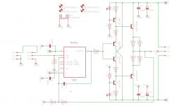
Simple diamond buffer based on a WJ design. Enclosed in the feedback loop of an OPA827.
DB open loop distortion is 0.0006xx% THD20 at 2Vrms into a 250 Ohm load.
Enclosed in the OPA827 feedback loop distortion is 0.000020%THD20 at 5Vrms into a 250 load. Note : I find this too optimistic, maybe the OPA827 model is too good?
Output transistor bias is set to 50mA, a little high, but gives very low distortion, even open loop.
Output transistors are the great KSC3503E/KSA1381E complementary pair from Fairchild. Usually used as VAS transistors, these highly linear TO-126 transistors are great for a headamp outputstage. Only downside is the 100mA(200mA pulsed) maximum collector current, but otherwise they work marvelously.
Using the KSC3503E/KSA1381E output pair, the design is good for 150-600 Ohm loads with extremely low distortion. Want to drive 32 Ohm loads? Use BD139/BD140 or similar.
Stable into 1pF-10nF capacitive loads.
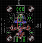
I went with a 4 layer PCB with Top Layer = Signal, Layer 2 = Power Ground Plane, Layer 3 = Power Plane, Bottom Layer = Signal.
It might be overkill, but the complete circuit is good to around 15MHz(-3dB) so I would rather be safe than sorry and besides, I have never done a 4 Layer PCB before so I might as well get some experience with it.
DB open loop distortion is 0.0006xx% THD20 at 2Vrms into a 250 Ohm load.
Enclosed in the OPA827 feedback loop distortion is 0.000020%THD20 at 5Vrms into a 250 load. Note : I find this too optimistic, maybe the OPA827 model is too good?
Output transistor bias is set to 50mA, a little high, but gives very low distortion, even open loop.
Output transistors are the great KSC3503E/KSA1381E complementary pair from Fairchild. Usually used as VAS transistors, these highly linear TO-126 transistors are great for a headamp outputstage. Only downside is the 100mA(200mA pulsed) maximum collector current, but otherwise they work marvelously.
Using the KSC3503E/KSA1381E output pair, the design is good for 150-600 Ohm loads with extremely low distortion. Want to drive 32 Ohm loads? Use BD139/BD140 or similar.
Stable into 1pF-10nF capacitive loads.
I went with a 4 layer PCB with Top Layer = Signal, Layer 2 = Power Ground Plane, Layer 3 = Power Plane, Bottom Layer = Signal.
It might be overkill, but the complete circuit is good to around 15MHz(-3dB) so I would rather be safe than sorry and besides, I have never done a 4 Layer PCB before so I might as well get some experience with it.
Attachments
Last edited:
discrete buffer in op amp loop sims do give seem to give disappointing numbers in my experience
especially when you could multiloop with the TPA6120 as output which are arguably quite a bit faster since they can have decades of current gain still @ ~100 MHz, and V gain too
compared to ft of the Q of only 150 MHz - current gain 1
especially when you could multiloop with the TPA6120 as output which are arguably quite a bit faster since they can have decades of current gain still @ ~100 MHz, and V gain too
compared to ft of the Q of only 150 MHz - current gain 1
The output stage heatsink in the current design is coupled to the Power Ground Plane and that in itself should give some decent thermal coupling between the output stage and driver stage transistors and ensure some form of bias stability but it might not be enough.
So one thing I thought about doing was mounting the output transistors horisontally on the PCB and use the PCB itself as cooling, should give better thermal coupling between the output stage and driver transistors for greater bias stability.
So one thing I thought about doing was mounting the output transistors horisontally on the PCB and use the PCB itself as cooling, should give better thermal coupling between the output stage and driver transistors for greater bias stability.
discrete buffer in op amp loop sims do give seem to give disappointing numbers in my experience
especially when you could multiloop with the TPA6120 as output which are arguably quite a bit faster since they can have decades of current gain still @ ~100 MHz, and V gain too
compared to ft of the Q of only 150 MHz - current gain 1
But where is the fun in that?
")
I know you really like that TPA6120 and I can definately see the appeal.
However I am not after beating these simple to use and inexpensive IC's, and the experience of designing something yourself, doing the schematic, layout, part selection etc is what makes this hobby interesting.
Will this design give me 0.0000xx& THD20 in real life? I highly doubt it, however, it will most likely give atleast below 0.001% THD20 at a full 5Vrms, 100mW into my 250 Beyerdynamics and if that is what I could get out of it, I would be more than happy. Note, the OPA827 in itself gives around 0.0002% THD20, 3Vrms into a 600 Ohm load at gain=1, so my goal of 0.001% THD20 at 5Vrms into a 250 Ohm load should be considered pretty conservative.
Now that I think about it, 0.0000xx THD20, at 5Vrms into 250 Ohm should be possible. Not that I expect to get it, but it should not be an impossibility.
Last edited:
- Status
- This old topic is closed. If you want to reopen this topic, contact a moderator using the "Report Post" button.