Hi All. Fresh from trying to sort out my RIAA phono stage, I discovered 2x new OPA2134 op amps and thought I would fit them to compare the DC offset at the output. Would you believe it...I STUPIDLY fitted one them reversed! My eyesight is very poor (I'm getting rather old) I didn't spot this until I switched the power on and it didn't work. I removed it and inserted it the correct way round and very surprisingly it worked...seemingly with no distortion but not able to do proper tests. However I'm not sure if I have damaged it as the offset is a negative voltage compared to the other one which was fitted OK. I was wondering though if the power supply +/- pins are protected internally with diodes?. Maybe someone has the circuit diagram schematic for this chip or someone might know?

They are not internally protected as such. They may survive reverse power, but you are never sure that the performance doesn't suffer.
For instance, they may look like working normally but have excessive noise.
I would Widlarize that chip, to avoid it will come back and haunt you ;-)
We still have a sign around our lab, "This is not a black-smith shop." But there were times when Bob would discover he had wasted a day or two, just because one bad part had screwed up his circuit. He would bring this bad part -- a capacitor, a pot, a transistor, an IC, or whatever -- over to the vise and lay it on the anvil part. Then he would calmly, methodically beat it with a hammer until the smallest remaining part was indistinguishable from the dust on the floor. Then he would go back to work and get the right answer. He explained that it makes you feel much better if you do this, and, you know that bad part will never come around again and goof you up. He was right. And I recommend that you join me in doing this "Widlarizing" when a bad component fools you. You will feel a lot better.
https://hackaday.com/2014/04/08/heroes-of-hardware-revolution-bob-widlar/
Jan
Thanks to all of you. I was very annoyed in that I had the chip for many years only to ruin it within a few seconds of putting it to use. Yes at the end of the day I'll just buy another one or three so I have at least a pair or 2 pairs of them. It will be interesting to see if any of the other new ones have a negative offset at the output. If none of them do...it will definitely have suffered some damage and will be binned. They are around £5 in the UK, not too much money, but my stupidity in making the mistake really bugs me 🙁 Love jan.didden's little story it made me laugh, I know the feeling well 🙂
The only way to not make mistakes, is to never do anything.
And even that can be a mistake.
And even that can be a mistake.
^ +1 to what @jan.didden says. Don't use it, it probably is impaired in some way or may suffer reliability issues in the future.
And just for curiosity, FET opamps like these should have really small offsets, I assume you are measuring just a millivolt or two for each chip?
And just for curiosity, FET opamps like these should have really small offsets, I assume you are measuring just a millivolt or two for each chip?
Charge it to the 'experience' account ;-)I was very annoyed in that I had the chip for many years only to ruin it within a few seconds of putting it to use.
Jan
As best I remember, a line by Jinx Shwartz from one of her novels: "Good judgement come from experience. A lot of experience comes from bad judgement."Charge it to the 'experience' account ;-)
🙂
Almost all chips have parasitic diodes between the positive and negative supply pins. Those are not meant to protect anything, they are just a consequence of putting a bunch of components in a common semiconducting substrate. Except for chip designs that are many decades old, there will probably also be ESD protection between the positive and negative supply, that is, some sort of power clamp and a big diode.I was wondering though if the power supply +/- pins are protected internally with diodes?. Maybe someone has the circuit diagram schematic for this chip or someone might know?
When you swap the positive and negative supplies and limit the current to < 100 mA, chances are that the chip survives. When the supply can supply many amperes, the chip will probably overheat. In between, I don't know.
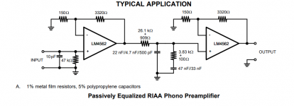
Hi Mooly. Thanks for asking. The undamaged one shows: 875mV...the presumably damaged one shows: -450mV. The pairs in each dual op-amp are connected in series with a passive RIAA filter in between but DC coupled via the 27kOhm resistor. With the filter, the gain is set to about 43db at 1KHz but I presume the gain at DC is exactly the sum of both amps so in my case is 63db (23+40...PLEASE NOTE I am using a higher gain (40db) on the 2nd stage than shown on the diagram)…then again there might be some loss through this filter resistor if DC flows here but not sure if it does. So, if we ignore any DC resistor loss, using an on-line calculator, 63db is a voltage ratio of 1413 times! So working backwards, the 875mV originates as 0.6mV and the neg 450mV starts off at approx. neg 0.3mV . I'm not an expert so I could be entirely wrong in how I worked out the INPUT off-set voltage. I would be very grateful if someone could let me know if the 0.6mV INPUT offset for the good OPA2134 seems about right or how to work out DC offset at the OUTPUT as the input offset figure is always shown on the spec sheets.. Much obliged.^ +1 to what @jan.didden says. Don't use it, it probably is impaired in some way or may suffer reliability issues in the future.
And just for curiosity, FET opamps like these should have really small offsets, I assume you are measuring just a millivolt or two for each chip?
Attachments
Last edited:
I think your calculations are fine but what does it tell us 🙂
Those total offset figures sound very high but in fact are entirely reasonable when you look at the circuit and its high DC gain from input through to output. I'm going to say its probably not an ideal configuration tbh but done to avoid any caps in the chain, whether those be coupling caps or caps in the feedback returns.
If you used something with high input bias currents (like a 5532) I'd bet the output would swing to one or other rail. It is very critical on opamps used as configured.
Hi Mooly. Yes I thought the same. The second stage ends up with a very big DC offset caused by the first stage amplifying its input offset and passing it on to be further amplified. A better design might be to have a trimming circuit on the first op-amp section to make sure there is no offset to feed into the 2nd stage? However I'm not sure a DUAL device is able to have this implemented? Otherwise maybe 2x individual OPA 134s in series might be the better way to do it...You are correct about the effect when using an NE5532...I fitted these and they show an offset of around 10.5V...surely they cannot operate properly if their circuit is "pulled over" to one side DC voltage wise? I would imagine they would clip asymmetrically very easily...and then act like a rectifier in effect when handling big voltage swings. Maybe a series blocking capacitor needs to be introduced after the filter to isolate the 2nd stage from the 1st stages DC output offset. It's hard to believe that TEXAS electronics never thought their design had a problem but then again it was using the LM4562 device. Hmmm... I'm ready to ditch this design I think 🙁I think your calculations are fine but what does it tell us 🙂
Those total offset figures sound very high but in fact are entirely reasonable when you look at the circuit and its high DC gain from input through to output. I'm going to say its probably not an ideal configuration tbh but done to avoid any caps in the chain, whether those be coupling caps or caps in the feedback returns.
If you used something with high input bias currents (like a 5532) I'd bet the output would swing to one or other rail. It is very critical on opamps used as configured.
Have you actually tried an LM4562? which is what the design is aimed at. That chip does have a much lower input offset voltage and also very low input bias currents. It may well be acceptable with that device.
I believe this would be a perfectly fine remedy. Alternately, with some added complication, you could apply a DC servo to drive the output to near 0V.A better design might be to have a trimming circuit on the first op-amp section to make sure there is no offset to feed into the 2nd stage?
- Home
- Amplifiers
- Solid State
- OPA134 / 2134 supply protection