I think you got GOLDFEEVER
Gold don't sound better, is not better for soldering, why gold?
Arne K
Gold don't sound better, is not better for soldering, why gold?
Arne K
About AP 1.7 with two supply boards - this means new production documentation and higher price. Probably it will be cheaper to buy 2 sets of AP1.7 in present version 😉
So all we need now is permission from Mr Pass - this is his project. I only designed PCBs basing on it 😉
So all we need now is permission from Mr Pass - this is his project. I only designed PCBs basing on it 😉
About AP 1.7 with two supply boards - this means new production documentation and higher price. Probably it will be cheaper to buy 2 sets of AP1.7 in present version
No problems on my part.
about the partslist, is there someone who can point to it? I seem to have some problem navigating Passlabs page 
Hello,
I would be interested in getting one set of the gold boards.
If it turns out that you end up getting the tin boards, I'd still would like to purchase one set of those, so count me in.
I'd prefer gold, though.
Best,
KT
I would be interested in getting one set of the gold boards.
If it turns out that you end up getting the tin boards, I'd still would like to purchase one set of those, so count me in.
I'd prefer gold, though.
Best,
KT
Only listening is boring ....😉
I need a new DIY project, this is a nice one.
So i would, if still possible, go for
- one set gold plated
- one psu
Grtz
Nick
I need a new DIY project, this is a nice one.
So i would, if still possible, go for
- one set gold plated
- one psu
Grtz
Nick
Hi!
If we get Nelson Pass Agreement, I update my order :
2 * P1.7 PCB
2 * PSU PCB
if not possible, i want as many 'sets' as necessary to get 2 PSU and I would prefer gold.
Perhaps It could be more acceptable by N. Pass if we just order PCBs (and no documentation...there is enough in Diyaudio.com).
In my humble opinion, this is DIY, so searching and understanding is part of the pleasure as much as building and listening.
Antoine
Hi guys!
I also want 2 psu and 4 main boards in gold if Nelson Pass will make his appointment to us! I hope so! Teake.
I also want 2 psu and 4 main boards in gold if Nelson Pass will make his appointment to us! I hope so! Teake.
Waiting for MR Pass permission I made some modifications on AP PCB's. I also decided to separate AP1.7 from supply board so dual mono is available now 😉
AP1.7 PCB
AP1.7 supply
AP1.7 PCB
AP1.7 supply
An externally hosted image should be here but it was not working when we last tested it.
Great news, Veteran🙂I also decided to separate AP1.7 from supply board so dual mono is available now
The boards look very nice😎
Steen.🙂
Count me in!
I'd be interested in two complete dual mono stereo sets, preferably gold (4 psu pcbs, 4 preamp pcbs).
Regards,
Scott
I'd be interested in two complete dual mono stereo sets, preferably gold (4 psu pcbs, 4 preamp pcbs).
Regards,
Scott
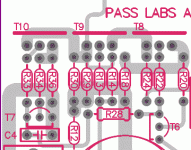
Taking a brief look at the pcb artwork, I got a little confused:
IRF610/9610's pinout is "GDS" (correct me if I am wrong), but here the gate resistors seem to be connected to the center pin.
Someone seems to have mixed up gate and drain - is it me or the board's designer...?
IRF610/9610's pinout is "GDS" (correct me if I am wrong), but here the gate resistors seem to be connected to the center pin.
Someone seems to have mixed up gate and drain - is it me or the board's designer...?
HBarske said:Taking a brief look at the pcb artwork, I got a little confused:
IRF610/9610's pinout is "GDS" (correct me if I am wrong), but here the gate resistors seem to be connected to the center pin.
Someone seems to have mixed up gate and drain - is it me or the board's designer...?
Everything is OK with the layout - my version of AP was tested by several people 😉 I draw transistors footprints above to show mounting holes and dimensions. Take a look at PCB from bottom:
An externally hosted image should be here but it was not working when we last tested it.
So yor actual layout isn't identical with the one posted on the first page of the thread?veteran said:Everything is OK with the layout
I attached a screenshot of that (early?) version, and that definintely has errors. R33, R13, R22 don't connect the FET's gate pins, as they should, following your schematic.
Attachments
- Status
- Not open for further replies.
- Home
- Group Buys
- (one more) ALEPH P 1.7 clone