I have found some components at the local junk yard lately 🙂
This is how it looks: 😀
Yes, I am building a gainclone with the LM3886 😎
Mabye a little oversized heatsink and power transformers for a normal two channel gainclone 😀
The powersupply was finnished last week...
This is how it looks: 😀
An externally hosted image should be here but it was not working when we last tested it.
An externally hosted image should be here but it was not working when we last tested it.
An externally hosted image should be here but it was not working when we last tested it.
An externally hosted image should be here but it was not working when we last tested it.
Yes, I am building a gainclone with the LM3886 😎
Mabye a little oversized heatsink and power transformers for a normal two channel gainclone 😀
The powersupply was finnished last week...
Need pcb-layout!
I recently became a member of a electronic-association for students, so now I can make my own pcb:s 🙂 That's cool!
I want to build a "normal gainclone", like BrianGT:s pcbs... But I want to make the pcb myself, it's more fun! 😉
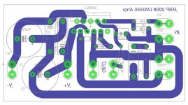
I'm looking for a board-layout: Non-inverted, single-sided for LM3886.
There are hundreds of layouts out there, some are made by newbies, and some by experienced people.
Of course I have searched, but its hard for me do decide a good layout.
I found a a layout made by "bigparsnip" here at the forum.
It is non inverted right? There are no errors right?
Shall I use it for my pcb:s?
What do you think?
I recently became a member of a electronic-association for students, so now I can make my own pcb:s 🙂 That's cool!
I want to build a "normal gainclone", like BrianGT:s pcbs... But I want to make the pcb myself, it's more fun! 😉
I'm looking for a board-layout: Non-inverted, single-sided for LM3886.
There are hundreds of layouts out there, some are made by newbies, and some by experienced people.
Of course I have searched, but its hard for me do decide a good layout.
I found a a layout made by "bigparsnip" here at the forum.
It is non inverted right? There are no errors right?
Shall I use it for my pcb:s?
What do you think?
Hi,
there is no RF attenuation nor chip decoupling on the PCB, nor DC blocking cap on the input.
The decoupling can easily be added directly to the chip power pins on the back of the PCB.
Similarly the RF cap can be paralleled with the Zin resistor on the back.
I don't like the common signal ground with the chip ground.
Similarly the Power Ground is commoned with the Signal Ground.
Either, select a layout with some or all of these features designed into the layout or be prepared to experiment with add ons after you have listened/measured the performance.
Okay, these things can easily be fixed, but not the other ones you mension...there is no RF attenuation nor chip decoupling on the PCB, nor DC blocking cap on the input.
The decoupling can easily be added directly to the chip power pins on the back of the PCB.
Similarly the RF cap can be paralleled with the Zin resistor on the back.
Is there a better layout out there? 🙂
Thank you! But there are things I don't understand...
There are both two inputs and outputs, Why? The LM3886 is inly one channel...
Edit: Now I get it 🙂 Found the schematic in eagle!
There are both two inputs and outputs, Why? The LM3886 is inly one channel...
Edit: Now I get it 🙂 Found the schematic in eagle!
This is the first attempt at PCB design and I am still figuring out eagle.
FYI, I made the board using toner transfer, but yet to build the amp.
So I cannot vouch for hum, ground loops etc.
Use at your own risk.
I tried to read and follow the info in previous posts on this forum when
doing the layout.
Feedback resistor is as close as possible to the chip.
The decoupling caps are as close as possible to the chip.
The power lines are on one side, closest to the chip.
The input signal is away from the power traces.
All traces are as thick as I could make them.
Attachments
DC coupled amplifier.
Where is the DC detect and output isolation?
No RF attenuation.
The decoupling caps are far too bulky and as a result had to be located too far from the power pins.
Look for 0.1inch or 0.2inch pin pitch for the 100nF decoupling.
NFB tied into the Power Ground instead of the Signal Ground.
Signal Ground sharing trace impedance with Power Ground.
I think I have found a good one now!
http://www.diyaudio.com/forums/showthread.php?threadid=65123
There is a small error, but it seems it's easy to correct in paint 🙂
http://www.diyaudio.com/forums/showthread.php?threadid=65123
There is a small error, but it seems it's easy to correct in paint 🙂
You can use my design, if you think it's appropriate for you.
http://www.diyaudio.com/forums/showthread.php?postid=1570826#post1570826
http://www.diyaudio.com/forums/showthread.php?postid=1570826#post1570826
Andrew, thanks for the feedback on the layout.
> DC coupled amp
The amp will be used with a preamp. I'll put in a coupling cap for safety.
> No RF attenuation.
There is an RC filter on the output. I wanted to avoid an inductor.
Others like BrainGT seem to follow the same.
> NFB tied into the Power Ground instead of the Signal Ground.
> Signal Ground sharing trace impedance with Power Ground.
Fixed now.
Decoupling caps are large, as that's what I have at hand now.
- Prasad
adding one DC blocking cap leaves the amp with mixed AC & DC coupling.quadtech said:Andrew, thanks for the feedback on the layout.
> DC coupled amp
The amp will be used with a preamp. I'll put in a coupling cap for safety.
> No RF attenuation.
There is an RC filter on the output. I wanted to avoid an inductor.
Others like BrainGT seem to follow the same.
I recommend you AC couple
or
DC couple with DC detect and output isolation.
There is no input RF attenuation. Fix it.
I have now etched my first board 😀
The second one didn't work out that well, so I will redo I on monday.
An externally hosted image should be here but it was not working when we last tested it.
The second one didn't work out that well, so I will redo I on monday.

Another Swedish DIY'er here
Hello!
Daniel sweden here!
I am new to the forum so I cant send Emails with it yet but could you please send me a mail at danielblixt(a)yahoo.se
/Daniel
Hello!
Daniel sweden here!
I am new to the forum so I cant send Emails with it yet but could you please send me a mail at danielblixt(a)yahoo.se
/Daniel
I printed the layout on a paper called laserstar.
Then I had uv-light, then NaOh, then etching...
I don't know what the method is called 🙂
Then I had uv-light, then NaOh, then etching...
I don't know what the method is called 🙂
An externally hosted image should be here but it was not working when we last tested it.
Two boards etched and the chips are mounted! Next thing to do is to order the components 🙂
- Status
- Not open for further replies.
- Home
- Amplifiers
- Chip Amps
- Olle:s first chipamp with LM3886! Board layout?