Hello all
I guess it is time to make it public.
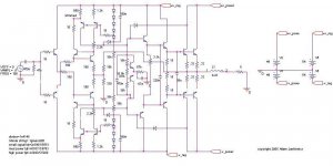
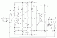
Below is the schematic of an amplifier I've built around 3 years ago but I don't have aby future plans about it.
The circuit is designed according to 'old school' fashion, namely: high OL bandwidth, relatively nice performance (THD, DF, bandwidth) before applying NFB loop, good PSRR and high output current.
But the 'novel circuit' part of the thread topic relates to, well.... just look!
I guess it is time to make it public.
Below is the schematic of an amplifier I've built around 3 years ago but I don't have aby future plans about it.
The circuit is designed according to 'old school' fashion, namely: high OL bandwidth, relatively nice performance (THD, DF, bandwidth) before applying NFB loop, good PSRR and high output current.
But the 'novel circuit' part of the thread topic relates to, well.... just look!
Attachments
This one has some nice features, some bad, but such circuits do sound pleasant in my experience, even if THD isn't extremaly low, say like 0.03%.
For your analysis.
For your analysis.
lumanauw said:Hi, darkfenriz,
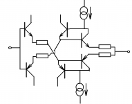
Is it CFB folded cascode amp?
Yes, I guess so, quite honestly the only CFB folded cascode amp I've ever seen.. 🙂
Adam,
It's a clever, ingenious design......
Distortion is low enough, the question is, does the distortion monotonically decrease with order?
Congratulations!!
Cheers,
Hugh
It's a clever, ingenious design......
Distortion is low enough, the question is, does the distortion monotonically decrease with order?
Congratulations!!
Cheers,
Hugh
Thanks, Hugh for kind words.
😉
David, this one has considerable offset drift (like +-130mV) and with just one rail it is rather rail-inefficient.
But these are issues I do not really care about, some others just do.
67k is there for limiting feedback factor for lower frequencies, this results in a little higher THD at low frequencies, but sliiiightly lower at higher frequencies. One reason for that is to keep the whole Otala-school and the other is that I wanted THD to be flat with frequency, rising with amplitude and lowering with harmonic order rather than very low overal THD number.
Of course everything will work OK without that 67k.
Regards
Adam
darkfenriz said:
Below is the schematic of an amplifier I've built around 3 years ago
but I don't have aby future plans about it.
.... the 'novel circuit' part of the thread topic relates to,
well.... just look!
I see your complementary input idea.
I like it 😎
... so much, that I will try to do some own Spice Testing of this.
( I have 2N5401 / 2N5551 and similar transistor models )
And I can compare this to old conventional ways to do inputs.
(We already seen too much many of those. They cant make Lineup raise eyebrows, not even 0.1 mm.)
Your amplifier idea is new to me.
Even if we can never know, if some clever did try this before.
🙂
Lineup
--------------
I attach a copy of your Basic Input Idea, using NPN + PNP transistors in complementary configuration
Attachments
AKSA said:Adam,
It's a clever, ingenious design ......
Cheers, Hugh
😎 I second that, Hughie Boy!!!
So now we are 2 good amplifier men 😉 saying same thing
about darkfenriz power amplifier schema
Lineup - has got this new idea to explore ... further
Hello All!!
I`ve opened a theme on Vegalab Óñèëèòåëü Adam Jankiewicz è åãî ìîäåðíèçàöèÿ and after some experiments with A. Jankiewicz amplifier and M-9 J. Roland I build an amlifier with perfect, amazing sound.
I`ve opened a theme on Vegalab Óñèëèòåëü Adam Jankiewicz è åãî ìîäåðíèçàöèÿ and after some experiments with A. Jankiewicz amplifier and M-9 J. Roland I build an amlifier with perfect, amazing sound.
Attachments

PCB in Sprint-Layot 5.0, biass carrent 100mA.Fully symmetric. Looks really nice.
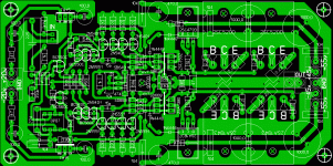
Can you share pcb layout and some more details?
Attachments
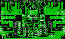
The PCB-s don't look like the schematic. Different components.
I checked the link you provide and there are several designs there.....similar between them.
Looks really promising for a future project.
In the schematic the input stage works with +/- 45 and the output with +/-35. Also the ground tracks look strange. The + and - rails each have a corresponding GND track. Can you explain how it works please...if it's not to much trouble.
- Status
- Not open for further replies.
- Home
- Amplifiers
- Solid State
- Old school, novel circuit amp