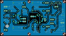
F1 and F2 may bump into your valve sockets if on the same side. The footprint looks small. Are you putting the valves on the same or opposite sides?
In that case fine. This may seem different from what others advise do put the boards next to each other. If they are far apart you can generate a differential ground current between the left and right coax braids on the input if they run over the power transformer. This will generate hum on both channels.
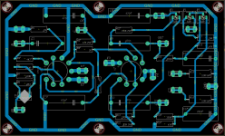
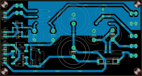
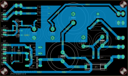
Initial version of the PSU PCB, again mostly copied from CB's version with the exception of a CRC snubber instead of the single capacitor.
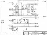
Schematic is available in post #22.
Also changed the ground trace around the board to a pour.
Thinking about whether I should build it as monoblocks or a stereo amp. I've got the 1669A which, atleast in terms of ratings, should be sufficient for a stereo pair.
Schematic is available in post #22.
Also changed the ground trace around the board to a pour.
Thinking about whether I should build it as monoblocks or a stereo amp. I've got the 1669A which, atleast in terms of ratings, should be sufficient for a stereo pair.
Attachments
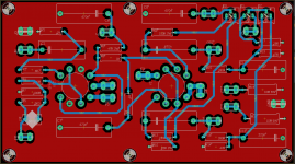
Might want to include the main rectifier negative trace into the ground pour. Trying to tie it strategically into the C negative terminal sounds good, but the shorter and more compact you make all rectifier traces the better. It is the most significant part of the layout for reducing 120Hz buzz.
Well spotted - Yep, don't take to the ground pour but to the cap directly so your circulating rectifier current does not enter the main ground. However since its on a separate PCB I cannot see a route for it getting into your main amp ground. On your amp schematic if you can get the ground the pour round the heaters that would help with the track winding its way around. Keep heater away from grid on first stage.
Last edited:
Thanks zigzagflux and badouin0.
For the rectifier trace, I was following what was done on the original board, although I did find it odd that it is taken to the bias cap and not the main filter cap.
I updated the pour on the PSU pcb, and for the amp PCB there are 2 options --
1. moving the traces a bit so that the pour can get around the heater
2. changing the layer of the ground.
which is preferred?
Attachments
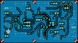
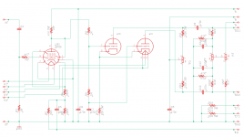
I think the blue one is ok up to you. My advise keep it away from the grid - you can get a buzz if there are rectifier components on the heater supply even 1pF can do this if your working with 100k impedance.
Are you referring to keeping the ground pour away from the grid? For the EF86, ECC83 or both?
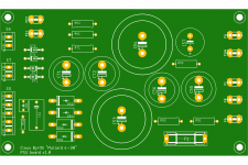
It would be a great help if you could annotate the image I attached, with arrows or circles, etc.
For PCB design, I am an absolute novice. I took a course on Eagle over at Udemy and that is what I have been using. For my purposes I have been very happy with it.
The only issue now is the subscription cost. I don't know how but apparently I got into some 1 year free trial when I initially installed it, but it has now expired and the cost is very high due to being bundled with Fusion360.
I am temporarily paying on a monthly basis to finish this project and may need to learn KiCad going forward.
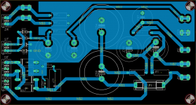
Pour is much improved. Could be a better physical layout, but the current density is better with shorter paths.
I would make N$1 as thick as possible as well.
Snubber is better across the AC line rather than across the DC line.
I would make N$1 as thick as possible as well.
Snubber is better across the AC line rather than across the DC line.
Oops! Thanks for catching that... I was totally intending the snubber before the rectifier as described in the Quasimodo paper.
I moved some of the caps around to make the board smaller, this is close to the best I will get it, I think.
N$1 is now 125mil, the rest are 100mil except the bias which is slightly less.
I moved some of the caps around to make the board smaller, this is close to the best I will get it, I think.
N$1 is now 125mil, the rest are 100mil except the bias which is slightly less.
Attachments
- Home
- Amplifiers
- Tubes / Valves
- Oh no... another Mullard 4-30 thread