Hi Guys
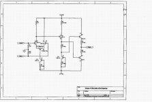
I am building this J-Fet OP Amp for my new line pre-amp project but I have problem to adjust the 50R trim pot to read 0 at the output. Instead I got +20V at the jointing point of the two 10R resistors. Does any one can tell me is there anything wrong in this circuit caused the error? Thanks
Chan
I am building this J-Fet OP Amp for my new line pre-amp project but I have problem to adjust the 50R trim pot to read 0 at the output. Instead I got +20V at the jointing point of the two 10R resistors. Does any one can tell me is there anything wrong in this circuit caused the error? Thanks
Chan
Attachments
Hi,
I don't have the skills to debug this problem, but a few more voltages appended to the schematic would help others find the fault.
Would de-sensitising the 50r pot help? Adding 100r to both sides of the pot and then adding 33r from each source to the wiper.
However, this is not a nice way to remove DC offset. It unbalances the LTP. Far better to trim the VAS bias current to adjust the voltage drop and current across the drain load R1.
I wonder if R1 is too low? what voltage is here?
I would use a matched pair of source resistors on the LTP (low to preserve gain) and then use these to check that LTP currents are really balanced (using the VAS trim)
Hi,
one extra measurement is not nearly enough.
But that 3V confirms 3mA into one half of the LTP.
Because you cannot check the source resistor currents you cannot check the LTP balance and you cannot check the total tail current =stumped!
I suspect that one half of the LTP is turned off or nearly so.
Give us more voltages. We can use them to calculate what currents are flowing around your circuit.
Could you remove the 50r pot and temporarily insert a pair of 24r resistors?
Hi Andrew
Could you remove the 50r pot and temporarily insert a pair of 24r resistors?
Do you mean insert a pair of 24R resistors and connect both to the S pins of Q1 & Q2? If so where should I connect the D pin of Q3. Please advice. Thanks
Could you remove the 50r pot and temporarily insert a pair of 24r resistors?
Do you mean insert a pair of 24R resistors and connect both to the S pins of Q1 & Q2? If so where should I connect the D pin of Q3. Please advice. Thanks
Hi,
CCS drain to junction of the two source resistors.
All I'm suggesting is removing the adjustable source resistors and replacing them with fixed resistors. That allows you to take useful measurements.
CCS drain to junction of the two source resistors.
All I'm suggesting is removing the adjustable source resistors and replacing them with fixed resistors. That allows you to take useful measurements.
First off, what do you have the inputs and outputs connected to?
Do you have a FEEDBACK resistor present?
A resistor to GROUND at one of the inputs?
The circuit might benefit from the addition of a jfet current mirror on top of the LTP... fwiw.
The Idss of the 2SJ74 (did you find a source for the exact part numbers? curious about that) in the second stage should likely be higher than the Idss of the 2SK170. That way the 170 will control the quiescent current of the 74. If it is the other way, the lower device will have little effect...
Looking at the circuit, the voltage wrt ground on either side of R3 should be about equal and close to ground... that creates slight bias and drive for the ouput devices...
The +20vdc tells you which way your circuit is being "pulled." Then look for the source of the driving voltage back in the circuit.
If you disconnect the gate of the 2SJ74 in the second stage, the output should be low in DC offset...
The current through the upper JFET, and the lower Jfet in the second stage by definition need to be about equal - the input pair provides the reference voltage to the upper JFET, there's a clue.
Of course, the opamp needs to be referenced to ground and have loop feedback first.
_-_-bear
Hi bear,
1. I have a 10R resistor connected to the +input (R9 at the circuit).
2. I use 2SK170BL & 2SJ74BL JFets. Is this pair good enough for this circuit?
3. Voltage at both sides of R3 is +22V.
4. Which point should I measure to get the reading of the current of the upper and lower JFets in the second stage?
5. Attached is the input/output schematic I used for this OP Amp.
Sorry for my question as I do not familiar with electronic theory.
Attachments
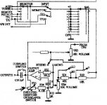
HKC said:1. I have a 10R resistor connected to the +input (R9 at the circuit).
Connect BOTH inputs to ground for testing, since this is a differential input, single ended output circuit.
C18 is series connected regarding feedback loop, so negative feedback won't be able to correct any DC errors on ouput, becouse C18 will pass thru AC signal only. Correct me if I'm wrong...
the trimmer has the function to allow to reduce the Vos to zero only, the opamp's problem is other. Infact, for a regular working it's necessary an appropriated selection of Q3 and Q4. The jfets selection is made in order to achieve that the voltage on the R4 is is comprised between 3X or 4x of the R2 voltage.....but it's possible avoid this uncheap and useless jfet selections adding one or two other trimmers in series to R2 and/or R4. In theory the Q3 and Q4 selections should be made basing on Q6 selection.
However, It's possible a short procedure to resolve the problem.
However, It's possible a short procedure to resolve the problem.
Hi peufeu
Thank you for your kind advice.
Yes you are right it is a differential input circuit but I think it is not a single end. Please correct me if I am wrong.
Best Regards
Thank you for your kind advice.
Yes you are right it is a differential input circuit but I think it is not a single end. Please correct me if I am wrong.
Best Regards
aparatusonitus said:C18 is series connected regarding feedback loop, so negative feedback won't be able to correct any DC errors on ouput, becouse C18 will pass thru AC signal only. Correct me if I'm wrong...
Exactly!!
JFETs need some DC current for gates. 1meg resistor parallel to C18 should cure the problem.
Hi darkfenriz
I connected a 1 Meg resistor parallel to C18 but the DC still exist. I still got +20V at the output.
I connected a 1 Meg resistor parallel to C18 but the DC still exist. I still got +20V at the output.
Looks like a serious problem.
I suspect you might have broken these Jfets because of exceeding maximum gate-drain voltage.
I suspect you might have broken these Jfets because of exceeding maximum gate-drain voltage.
Hi darkfenriz
Sorry I made a mistake, it works now. I can adjust the output voltage to read 0. Thanks
Sorry I made a mistake, it works now. I can adjust the output voltage to read 0. Thanks
Hi Darkfenriz
I am having the following situation right now:
1. With the 1 Meg resistor added parallel to C18 I got very loud dee dee noise but I can adjust the output to zero.
2. Replace the 1 Meg resistor with a 20K the dee dee noise is lower and the output can not be adjusted to absolute zero.
3. without any resistor added, I got +20V at the output but no dee dee noise.
Please advice why this happen and any thing can be done to solve the noise problem?
Thanks again
Hi Mlloyd
Thank you for sending the web information of Fred. I am going to send an e-mail hope he can help to solve the problem.
Thank you for sending the web information of Fred. I am going to send an e-mail hope he can help to solve the problem.
This circuit has a serious issue, 2SJ74 has max Vds rating of 25v. Max voltage supply should be +/-12v, not 24v.
Mike
Mike
- Status
- Not open for further replies.
- Home
- Amplifiers
- Solid State
- Offset of JFet OP Amp