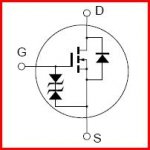
External zeners do indeed clamp. The laterals have a built in zener as PA says like this (see pic). I suspect your latching on a lateral is more to do with the device becoming overheated and going into some kind of runaway. At 160 degrees case temp the die temp will be hotter still.
Other types of FET do not have inbuilt zener clamps or "static" clamp diodes as if these were incorporated onto the die they would cause the device to latch under certain conditions. Their addition makes the device a type of thyristor if they were ever triggered into conduction. Once triggered the device can't be controlled by the gate and if sufficient current flows it would be destroyed.
Other types of FET do not have inbuilt zener clamps or "static" clamp diodes as if these were incorporated onto the die they would cause the device to latch under certain conditions. Their addition makes the device a type of thyristor if they were ever triggered into conduction. Once triggered the device can't be controlled by the gate and if sufficient current flows it would be destroyed.
Attachments
Thanks for that explanation 🙂
The strange thing about the latching I observed is that the transistor turns off. If the current in the gate is kept up the gate is still latched to source when the transistor cools down due to being turned off. Turning off Vds has no effect on the latching, only turning off the current into the gate unlatches the transistor.
The strange thing about the latching I observed is that the transistor turns off. If the current in the gate is kept up the gate is still latched to source when the transistor cools down due to being turned off. Turning off Vds has no effect on the latching, only turning off the current into the gate unlatches the transistor.
Hey, don't forget class D audio, latest generation IR verticals are very hard to beat in these applications 😀
Jacco,
Fast and linear. OK, not quite like verticals.Rds(on) = 10 Ohm for the TO-220. (Mr Peter Walker would turn around in his grave if he heard talks about fast current dump devices)
Sidenote :
the Rds(on) of 10 Ohm that i mentioned is the value printed on '80s paper.
As in paper datasheets. ( it's paper. Have you ever seen paper ? ©Waterworld)
Spice models of the Hitachi J7*/K21* series use an Rds(on) value of 6 Ohm.
20W semi-lateral Toshiba 2SJ313/2SK2013 have an Rds(on) of 5 ohm, so the Hitachi value will be at least 6 Ohm, but who cares really.
megajocke said:Thanks for that explanation 🙂
The strange thing about the latching I observed is that the transistor turns off. If the current in the gate is kept up the gate is still latched to source when the transistor cools down due to being turned off. Turning off Vds has no effect on the latching, only turning off the current into the gate unlatches the transistor.
Sounds like it's going open circuit drain to source if your saying no current flows but you still have gate voltage present (if any DC current is flowing into or out of the gate the poor thing is well zonked). All sorts of weird things can happen at extreme temperatures and even if it appears O.K. on cooling I wouldn't use it for anything after that.
No there isn't any gate voltage as the gate and source clamp together. It's like there is a thyristor between gate and source that triggers on high temperature. Gate voltage drops to 0.7V or so (gate resistors limit the current) so the drain-source current drops pretty low.
The current flowing into the gate (or is it the internal zeners doing something strange?) won't go away just by cooling down, it's just like a thyristor. And I can't see how the gate current could keep anything internal hot - it's like 5mW of power!
Now this probably isn't something that should be relied on in normal operation but it sure is better than blowing the output stage on overload...
Hi,
I guess we will never know 🙂 The tests would have to be repeated under controlled conditions and anyway, once the maximum die temperature or any other parameter has been exceeded even momentarily all bets are off.
I guess we will never know 🙂 The tests would have to be repeated under controlled conditions and anyway, once the maximum die temperature or any other parameter has been exceeded even momentarily all bets are off.
I'm going to try this on the other 3 I have I think. (I got them for free and in this strange package I won't build an amp with them - impossible to repace if I break them) I'll try building a simple amp when I get home in a couple of weeks and see if I can blow it up by overloading it. 😀
But it seems like others have observed this behaviour too - amps using these are known for being almost impossible to blow up.
But it seems like others have observed this behaviour too - amps using these are known for being almost impossible to blow up.
I've been playing hard with a couple of pairs of lateral monoblocks today. Getting them to output full-power sinewaves while I measured THD, hitting them with squarewaves, driving them hard into clipping, all into my thumper 8 ohm load. The load was hot, the heat sink the monoblocks was bolted to was almost too hot to touch.
Before starting I'd biased them to 100mA per device and set the offset under 1mV. After I'd finished while everything was still stinking hot I thought I'd measure bias and offset to see how they were tracking. All the FETs were within a few milliamps of 85mA, and offset had gone out to nearly 5mV.
Do that with bipolar parts!
agreed! Here I have a 2x500W Block from the eighties with 6x2SJ49/2SK134 each channel that serves as a lab test amp.I've been playing hard with a couple of pairs of lateral monoblocks today. Getting them to output full-power sinewaves while I measured THD, hitting them with squarewaves, driving them hard into clipping, all into my thumper 8 ohm load. The load was hot, the heat sink the monoblocks was bolted to was almost too hot to touch.
Before starting I'd biased them to 100mA per device and set the offset under 1mV. After I'd finished while everything was still stinking hot I thought I'd measure bias and offset to see how they were tracking. All the FETs were within a few milliamps of 85mA, and offset had gone out to nearly 5mV.
Do that with bipolar parts!
These FETs are really bullet-proof!🙂
I've been playing hard with a couple of pairs of lateral monoblocks today. Getting them to output full-power sinewaves while I measured THD, hitting them with squarewaves, driving them hard into clipping, all into my thumper 8 ohm load. The load was hot, the heat sink the monoblocks was bolted to was almost too hot to touch.
Before starting I'd biased them to 100mA per device and set the offset under 1mV. After I'd finished while everything was still stinking hot I thought I'd measure bias and offset to see how they were tracking. All the FETs were within a few milliamps of 85mA, and offset had gone out to nearly 5mV.
Do that with bipolar parts!
Nice results. Lateral MOSFETs are indeed probably the most temperature stable of output devices. A 15% change in bias level from cold to quite hot is very good, and can probably only be done with ThermalTrak bipolar output devices in a carefully-designed circuit. What's more, MOSFETs are much more tolerant of bias changes anyway, since there is no Barney Oliver biasing criteria involved. Vertical MOSFETs are also very good in this regard, although slightly more temperature sensitive than laterals, since the onset of their negative temperature coefficient occurs at a significantly higher bias current than is normally used.
I recently did a redesign of a Hafler DH220 and got very good results. I biased each output device at 200mA.
Cheers,
Bob
Most of that offset drift with higher temperature is attributable to drift in the parameters of the input stage.I've been playing hard with a couple of pairs of lateral monoblocks today. Getting them to output full-power sinewaves while I measured THD, hitting them with squarewaves, driving them hard into clipping, all into my thumper 8 ohm load. The load was hot, the heat sink the monoblocks was bolted to was almost too hot to touch.
Before starting I'd biased them to 100mA per device and set the offset under 1mV. After I'd finished while everything was still stinking hot I thought I'd measure bias and offset to see how they were tracking. All the FETs were within a few milliamps of 85mA, and offset had gone out to nearly 5mV.
Do that with bipolar parts!
I don't think you can blame the latFETs for that.
Same with a BJT output stage. Most of the drift in output offset is attributable to the input stage.
It's the NFB that ensures this is so.
The NFB cannot correct for changes between the two input transistors.
This is why D.Self, R.Cordell and others measured and reported what happens when the input stage is not carefully balanced.
but it is still a very good result for output offset drift, where no DC servo has been used. A change from near zero offset to 5mVdc offset is very good for a worst case condition.
Last edited:
I've spent the day measuring an amp built with Exicon Lateral MOSFETS (ECX10N20 & ECX10P20) rather than my usual Renesas parts.
No issues with stability compared to the Renesas parts - no need whatsoever for any changes to the PCB - just whack the Exicon parts in. Distortion performance is pretty-much the same, though doing a really good measurement to show any difference will really take a little while.
One unexpected difference, and something that I quite like, is that the Vgs(th) has a stronger negative temperature coefficient than for the Renesas parts. In practice if I set a pair of Renesas Laterals up to 50mA bias, I'll come back and measure it once it's stabilised at ~70mA. It's not a big thing, but it does put a lower bound on useable quiescent current. The Exicon ones I can set to whatever I like and they stay put.
It's a subtle difference, but one which makes them more amenable to low quiescent low-power amps, like for example a tweeter driver in a multi-way amp.
Interesting, have you any off the original Hitachi? I have 6 amps with Hitachi fets, 4 modern driven by the LM49830 chip and 2 old 80's maplin amps where one transistor is substituted with the Renesas equivalent I believe. Possibly the Exicon is better that the Hitachi
My understanding is that the only difference between Hitachi and Renesas is the branding. Hitachi spun off their semiconductor business to form Renesas.
Of course there may be differences between the product due to fab improvements over the years.
I just looked up the data sheet for the Exicon parts. They claim the zero tempo point is about 100mA, so not as I was measuring.
Of course there may be differences between the product due to fab improvements over the years.
I just looked up the data sheet for the Exicon parts. They claim the zero tempo point is about 100mA, so not as I was measuring.
You can add the ALFET (from Magnatech - part of Semelab TT electronics) branded Lateral Mosfets to the EXICON types as all being much the same product as the remaining RENESAS Latfets. Both these alternative brands were once also supplied in double and single die variants in plastic and TO3 packages with standard and higher voltage types for more powerful arrays, whether double or single die packages. However, the brand has recently become scarce and seems to be going the way of the dodo.
Exicon = Renesas = Semelab
Pretty much a branding thing.
You can use different source resistor values vs the Hitachi parts too with those brands.
Latfets make sense to me, not that there aren't good designs either way...
Pretty much a branding thing.
You can use different source resistor values vs the Hitachi parts too with those brands.
Latfets make sense to me, not that there aren't good designs either way...
- Status
- Not open for further replies.
- Home
- Amplifiers
- Solid State
- Ode to Lateral MOSFETs