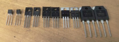
Cheap OEM pots go bad , but hermetically sealed Bourns trimmers are
aerospace quality (20 years +).
Offset is nice , if it is external (DC injection). LTP is rarely a perfect match.
You need bias.
CSS adjust can .... be good. BJT's have a current "sweet spot" of highest gain.
Yes ,Wolverine is mine (Badger/blameless ++)
To beat the other amps , not covered in depth by many.
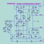
Other amps are the Leach amp. You can do it very simple (below 1).
That symmetric will cancel out thermally minus the error of the gain difference
between 1st/2nd stages. Pretty good.
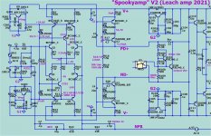
(below 2) is one that is accurate .05mA 0-70C. Hawksford VAS is unique at
clip , LED flash !! and prevent any overload Q11-14. Clip looks rounded
like a tube amp and is much harder to hear. TOP dog , but simple.
PS , a "blameless" will beat it at 20Khz but not in durabilty or PSRR. (or sound).
20hz-10Khz they are the same.
OS
aerospace quality (20 years +).
Offset is nice , if it is external (DC injection). LTP is rarely a perfect match.
You need bias.
CSS adjust can .... be good. BJT's have a current "sweet spot" of highest gain.
Yes ,Wolverine is mine (Badger/blameless ++)
To beat the other amps , not covered in depth by many.
Other amps are the Leach amp. You can do it very simple (below 1).
That symmetric will cancel out thermally minus the error of the gain difference
between 1st/2nd stages. Pretty good.
(below 2) is one that is accurate .05mA 0-70C. Hawksford VAS is unique at
clip , LED flash !! and prevent any overload Q11-14. Clip looks rounded
like a tube amp and is much harder to hear. TOP dog , but simple.
PS , a "blameless" will beat it at 20Khz but not in durabilty or PSRR. (or sound).
20hz-10Khz they are the same.
OS
Attachments
Cheap OEM pots go bad , but hermetically sealed Bourns trimmers are
aerospace quality (20 years +).
Offset is nice , if it is external (DC injection). LTP is rarely a perfect match.
You need bias.
CSS adjust can .... be good. BJT's have a current "sweet spot" of highest gain.
Yes ,Wolverine is mine (Badger/blameless ++)
To beat the other amps , not covered in depth by many.
Other amps are the Leach amp. You can do it very simple (below 1).
That symmetric will cancel out thermally minus the error of the gain difference
between 1st/2nd stages. Pretty good.
(below 2) is one that is accurate .05mA 0-70C. Hawksford VAS is unique at
clip , LED flash !! and prevent any overload Q11-14. Clip looks rounded
like a tube amp and is much harder to hear. TOP dog , but simple.
PS , a "blameless" will beat it at 20Khz but not in durabilty or PSRR. (or sound).
20hz-10Khz they are the same.
OS
Hey that's awesome!! (Wolverine).
I am presently implementing simpler concepts that can still deliver a compelling audio quality, and will surely explore beyond that soon - A step at a time. This is my first project in a long time, and the first time I've ever done a PCB layout.
Hmmm... after your comment on the symmetric layout and its not too significant impact on audio quality, I am now getting inclined to move the speaker output back to where it was originally - Away from the NFB 🙂
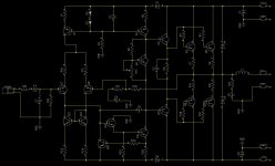
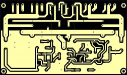
No , if study my type layout carefully ... you will see P/N/P/N alternating.
I takeoff NFB between a P/N pair (right in the middle-of just one pair).
The other 2 pair P/N's don't matter. My output coil (L1) also comes right from the middle
of the farthest right P/N pair.
Just taking NFB from the middle and having L1 at the end will either disrupt
P or N at the centered NFB point.
Even as I am not globally symmetric , my L1 and NFB is perfectly symmetric.
PS - the other "symmetric" is the actual design of the amp. A symmetric
IPS is one with opposing LTP/VAS , like a Leach amp. Totally different
than output stage symmetry , either physical or NFB wise.
ostripper, what is the function of U1, 4N25?
Microprocessor bias external control with a passive default.
Set (passive default) to 50mA , OPTI 1 can step up to 150mA with
a 4-bit word.
OPTO fully isolates the high Z 110V p-p Vbe circuit from the (LED).
control.
A multi-position switch or switch/pot could be on the front panel -
100K = 75mA to 39K= 150mA. Open circuit opto led would be default.
OS
No , if study my type layout carefully ... you will see P/N/P/N alternating.
I takeoff NFB between a P/N pair (right in the middle-of just one pair).
The other 2 pair P/N's don't matter. My output coil (L1) also comes right from the middle
of the farthest right P/N pair.
Just taking NFB from the middle and having L1 at the end will either disrupt
P or N at the centered NFB point.
Even as I am not globally symmetric , my L1 and NFB is perfectly symmetric.
PS - the other "symmetric" is the actual design of the amp. A symmetric
IPS is one with opposing LTP/VAS , like a Leach amp. Totally different
than output stage symmetry , either physical or NFB wise.
Oh Wow - I actually did miss the P/N/P/N alternating layout. Interesting!
So then I will stay put on the (+) speaker output placement, and try to place the inductor as far as I can from the NFB. The vertical mounting of the inductor should help to some extent in reducing the inductive coupling with adjoining components.
Yes I now understand the other "symmetric" design that you pointed out 🙂
The Latest:
Removal of the ground plane will be a bit more involved since it will require a ground trace running through the PCB. Presently the ground plane takes case of ground for a few components. So keeping the ground plane as of now.
Removal of the ground plane will be a bit more involved since it will require a ground trace running through the PCB. Presently the ground plane takes case of ground for a few components. So keeping the ground plane as of now.
Attachments

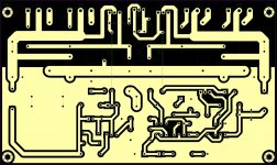
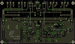
Updated PCB traces to make the Speaker takeoff point same as the NFB takeoff point (both from the middle of the output trace). Hopefully, this ghost has now been laid to rest.
What is left is to add a damping resistor across the output inductor. Yes, that got missed in the schematic as well, and will be added to both the schematic as well as the PCB Layout. Thank you Nick Cresswell (chefhat) for pointing out this error!
What is left is to add a damping resistor across the output inductor. Yes, that got missed in the schematic as well, and will be added to both the schematic as well as the PCB Layout. Thank you Nick Cresswell (chefhat) for pointing out this error!
Attachments
Last edited:
Oak Leaf - YABI (Yet Another Blameless Implementation)
Version 1.5.1
a). Added damping resistor (R27) across output inductor (L1).
L1 will be vertically mounted and the resistor will also be vertically mounted inside of it.
b). Re-routed NFB track to make it smaller in length.
Version 1.5.1
a). Added damping resistor (R27) across output inductor (L1).
L1 will be vertically mounted and the resistor will also be vertically mounted inside of it.
b). Re-routed NFB track to make it smaller in length.
Attachments
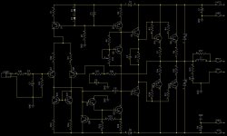
Oak Leaf - Now is when the rubber meets the road
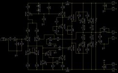
At the very outset (first post of this thread), I had mentioned the broad design goals for this amplifier build, and and also that I have picked the simplest concepts for each stage (Input/VAS/Output) from various books, that I believe, would work well together to meet those goals.
Now the real fun starts, or as they say - Now is when the rubber meets the road - Finalizing the schematic. This requires fleshing out the concepts with actual components/values.
Since my experience in audio is limited (putting it mildly), I'm sure there will be several improvement areas that I'm hoping would get pointed out.
I am now sharing the initial schematic that I have in mind which of course is open to perusal/corrections of any shortcomings (keeping the goals in mind).
Let me re-iterate the goals in this post as well for easy reference:
1). 150W RMS Power into 8 Ohms.
2). 4 Ohms driving capability (I believe that would be 260W into 4 Ohms).
3). THD within 0.05% at 250W RMS at 4 Ohms and 20KHz.
4). Least number of components to achieve the above.
I am open to discussing the above goals as well if anyone thinks that any need to be re-considered.
Attachments
Last edited:
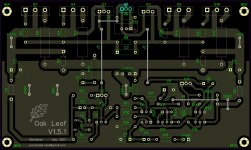
Almost there.
Your common returns (6 in total) need to be segregated. I suppose it's a bit of a headache, but the most difficult is to start. Speaker return (the 7th return) should go straight to the power supply common (assuming you won't bring the whole power supply onto the AMP PCB)
Your common returns (6 in total) need to be segregated. I suppose it's a bit of a headache, but the most difficult is to start. Speaker return (the 7th return) should go straight to the power supply common (assuming you won't bring the whole power supply onto the AMP PCB)
Almost there.
Your common returns (6 in total) need to be segregated. I suppose it's a bit of a headache, but the most difficult is to start. Speaker return (the 7th return) should go straight to the power supply common (assuming you won't bring the whole power supply onto the AMP PCB)
Thank you for the inputs!
I understand what you are saying is relevant for the PCB layout.
Unfortunately, when I made this PCB layout, it was designed ground up (pun intended) for using the ground plane for supplying ground to all components (Yep a clanger. I know better now).
I was just wondering if I can stick in several ground wires from the power supply to the board at strategic places (maybe like 3 or 4 places) and get away with it?
Yes, the speaker return can actually be removed from the board and come off the power supply common. That would actually help take some high currents off the ground plane. Only high currents that will remain will be at the two ends of the PCB that supply current to the output stage which can have their own ground wires from the power supply.
Tell me it will work... please.... 🙂
Last edited:
Have a look here:
A Complete Guide to Design and Build a Hi-Fi LM3886 Amplifier - Circuit Basics
https://www.circuitbasics.com/wp-co...er-With-an-LM3886-Master-Wiring-Diagram-4.png
Also - see attached photo
A Complete Guide to Design and Build a Hi-Fi LM3886 Amplifier - Circuit Basics
https://www.circuitbasics.com/wp-co...er-With-an-LM3886-Master-Wiring-Diagram-4.png
Also - see attached photo
Attachments

Have a look here:
A Complete Guide to Design and Build a Hi-Fi LM3886 Amplifier - Circuit Basics
https://www.circuitbasics.com/wp-co...er-With-an-LM3886-Master-Wiring-Diagram-4.png
Also - see attached photo
Now that's certainly a subtle hint as to what needs to be done 😉
Wonderful links there - Thanks!
Now that you (and a few others before you who essentially pointed out the same thing) got me thinking on the grounding aspect, I did a bit of lookup on the topic and it seems there is another interesting topology other than the star ground that is demonstrated in the PCB image you shared.
Bob Cordell BC 1 BAF 2019 Final - YouTube
This is a deep link half an hour into Bob Cordell's presentation at Burning Amp 2019 where he talks about the power and grounding topology that he used for the BC-1.
This certainly seems more "PCB Trace Layout Friendly" then the star ground topology with "medusa hair" traces moving all across the board.
What do you feel?
Attachments

Attachments
Grounding-reg
Nice Layout, but your grounding scheme requires refinement.
All ground traces should come to a single pint on the pcb, where you will connect the 0V line.
Speaker return can be removed from the pcb and connected directly to the PSU ground, the center of the filter caps.
Route the signal ground, decoupling cap grounds, NFB ground separately and make all grounds meet at a single point. Also include a 10R ground lift resistor between Mani ground and signal ground.
Thanks,
sumesh
The Latest:
Removal of the ground plane will be a bit more involved since it will require a ground trace running through the PCB. Presently the ground plane takes case of ground for a few components. So keeping the ground plane as of now.
Nice Layout, but your grounding scheme requires refinement.
All ground traces should come to a single pint on the pcb, where you will connect the 0V line.
Speaker return can be removed from the pcb and connected directly to the PSU ground, the center of the filter caps.
Route the signal ground, decoupling cap grounds, NFB ground separately and make all grounds meet at a single point. Also include a 10R ground lift resistor between Mani ground and signal ground.
Thanks,
sumesh
Thank You!
Yes, the ground topology (or rather the lack of it) has been pointed out by others too thanks to my ignorance on this subject when I did the initial layout.
I understand you are proposing the star grounding topology. Please do check post #35 above where another power and ground topology is put forward, and let me know your thoughts.
- Home
- Amplifiers
- Solid State
- Oak Leaf - YABI (Yet Another Blameless Design)